
 100% FREE ACCESS
12th Standard CBSE Syllabus & Materials
12th Standard CBSE
CBSE 12th Economics Government Budget and the Economy Previous year Question Papers Study Material - QB365 Set A
NEW12th Standard CBSE
CBSE 12th Computer Science Interface Python with MySQL - New Previous year Question Papers Study Material - QB365 Set A
NEW12th Standard CBSE
CBSE 12th Computer Science Database Concept - New Previous year Question Papers Study Material - QB365 Set A
NEW12th Standard CBSE
CBSE 12th Computer Science Data Communication - New Previous year Question Papers Study Material - QB365 Set A
NEW12th Standard CBSE
CBSE 12th Computer Science Data Structures - New Previous year Question Papers Study Material - QB365 Set A
NEW12th Standard CBSE
CBSE 12th Computer Science Functions - New Previous year Question Papers Study Material - QB365 Set A

Published on: 07/03/2026
Download CBSE Class 12th Standard CBSE Physics question papers, sample papers, important questions, and previous year solved papers in PDF format. Get free study materials, NCERT solutions, and exam preparation resources for Class 12th Standard CBSE Physics
Questions + Answers key
Take MCQ Physics Test
1.
From the relation R = R0A1/3, where R0 is a constant and A is the mass number of a nucleus, show that the nuclear matter density is nearly constant (i.e. independent of A).
2.
Find the energy equivalent of one atomic mass unit, first in Joules and then in MeV. Using this, express the mass defect of \({ }_{8}^{16} \mathrm{O} \text { in } \mathrm{MeV} / \mathrm{c}^{2}\)
3.
In half wave rectification , what is the output frequency if the input frequency is 50 Hz. What is the output frequency of a full wave rectification for the same input frequency.
4.
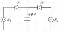
(i) In the following diagram, which bulb out of B1 and B2 will glow and why?
(ii) Draw a diagram of an illuminated p-n. junction solar cell.
(iii) Explain briefly the three processes due to which generation of emf takes place in a solar cell.
5.
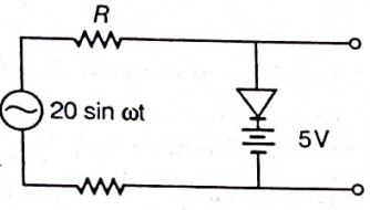
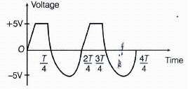
Assuming an ideal diode, draw the output waveform for the circuit given in the figure, explain the waveform.
6.
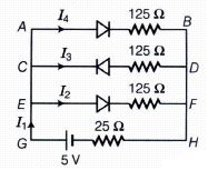
If each diode in figure has a forward bias resistance of \(25\Omega \) and infinite resistance in reverse bias, what will be the values of the currents \(I_{ 1 },I_{ 2 },I_{ 3 } \ and \ I_{ 4 }\) ?
7.
A neutron strikes \(_{ 5 }{ { B }^{ 10 } }\)nucleus with the subsequent emission of an alpha particle. What is the atomic number, mass number and chemical name of the remaining nucleus?
8.
A photon of wavelength \(3310\mathring { A } \)falls on a photocathode and an electron of energy \(3\times { 10 }^{ -19 }\)J is ejected. If the wavelength of the incident photon is changed to \(5000\mathring { A } \), the energy of the ejected electron is \(9.72\times { 10 }^{ -20 }\)J. Calculate the value of Planck's constant and threshold wavelength of the photon.
9.
The work function for cesium is 1.8eV. Light of \(4500\mathring { A } \) is incident on it. Calculate
(i) the maximum kinetic energy of the emitted photoelectron
(ii) maximum velocity of the emitted photoelectron
(iii) if the intensity of the incident light is doubled, then find the maximum kinetic energy of the emitted photoelectron
Given \(h=6.6\times { 10 }^{ -34 }Js,\ { m }_{ e }=9.1\times { 10 }^{ -31 }kg, \ c=3\times { 10 }^{ 8 }{ ms }^{ -1 }\)
10.
The electric field associated with a monochromatic beam of light becomes zero, \(2.4\times { 10 }^{ 15 }\) times per second. Find the maximum kinetic energy of the photoelectrons when this light falls on a metal surface whose work function is 2.0eV, h=\(6.63\times { 10 }^{ -34 }Js\)
11.
Using Bohr model, calculate the electric current created by the electron when the H-atom is in the ground state.
12.
What is the de-Broglie wavelength of a nitrogen molecule is moving with the root-mean-square speed of molecules at this temperature. (Atomic mass of nitrogen = 14.0076 u)
13.
From Bohr's atomic model, we know that the electrons have well defined energy levels in an isolated atom. But due to interatomic interactions in a crystal, the electrons of the outer shells are forced to have energies different from those in isolated atoms. Each energy level splits into a number of energy levels forming a continuous band.The gap between top of valence band and bottom of the conduction band in which no allowed energy levels for electrons can exist is called energy gap.
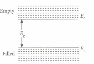
(i) In an insulator energy band gap is
| (a) Eg = 0 | (b) Eg< 3eV | (c) Eg > 3eV | (d) None of the above |
(ii) In a semiconductor, separation between conduction and valence band is of the order of
| (a) 0 eV | (b) 1 eV | (c) 10 eV | (d) 50 eV |
(iii) Based on the band theory of conductors, insulators and semiconductors, the forbidden gap is smallest in
| (a) conductors | (b) insulators | (c) semiconductors | (d) All of these |
(iv) Carbon, silicon and germanium have four valence electrons each. At room temperature which one of the following statements is most appropriate?
| (a) The number of free electrons for conduction is significant only in Si and Ge but small in C. |
| (b) The number of free conduction electrons is significant in C but small in Si and Ge. |
| (c) The number of free conduction electrons is negligibly small in all the three. |
| (d) The number offree electrons for conduction is significant in all the three. |
(v) Solids having highest energy level partially filled with electrons are
| (a) semiconductor | (b) conductor | (c) insulator | (d) none of these |
1.
We have the expression for nuclear radius as:
R = R0A1/3
Where,
R0 = Constant.
A = Mass number of the nucleus
Nuclear matter density, \(\rho \ =\frac{Mass\ of\ the\ nucles}{Volume\ of\ the\ nucles}\)
Let m be the average mass of the nucleus.
Hence, mass of the nucleus = mA
\(\therefore \rho=m \frac{A}{\frac{4}{3} \pi R^{3}}=\frac{3 \mathrm{~mA}}{4 \pi\left(R_{0} A^{\frac{1}{3}}\right)^{3}}=\frac{3 m A}{4 \pi R_{0}^{3} A}=\frac{3 \mathrm{~m}}{4 \pi R_{0}^{3}}\)
Hence, the nuclear matter density is independent of A. It is nearly constant.
2.
1u = 1.6605 x 10⁻²⁷ kg
To convert it into energy units, we multiply it by c2 and find that energy equivalent = \(1.6605 \times 10^{-27} \times\left(2.9979 \times 10^{8}\right)^{2} \mathrm{~kg} \mathrm{~m}^{2} / \mathrm{s}^{2}\)
\(=1.4924 \times 10^{-10} \mathrm{~J}\)
\(=\frac{1.4924 \times 10^{-10}}{1.602 \times 10^{-19}} \mathrm{eV}\)
\(=0.9315 \times 10^{9} \mathrm{eV}\)
\(=931.5 \mathrm{MeV}\)
or, \(1 \mathrm{u}=931.5 \mathrm{MeV} / \mathrm{c}^{2}\)
For, \({ }_{8}^{16} \mathrm{O}, \quad \Delta M=0.13691 \mathrm{u}=0.13691 \times 931.5 \mathrm{MeV} / \mathrm{c}^{2}\)
\(=127.5 \mathrm{MeV} / \mathrm{c}^{2}\)
The energy needed to separate \({ }_{8}^{16} \mathrm{O}\) into its constituents is thus 127.5 MeV/c2.
3.
Given, input frequency = 50 Hz
For a half-wave rectifier, the output frequency is equal to the input frequency.
\(\therefore\) Output frequency = 50 Hz
For a full-wave rectifier, the output frequency is twice the input frequency.
\(\therefore\) Output frequency = 2 x 50 = 100 Hz.
4.
(i) D1 diode is forward biased, hence current will flow in B1 bulb and D2 is reverse biased, so there will be no current in B2. Hence, BI will glow.
(ii) The diagram of illuminated p-n junction solar cell is given below
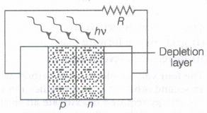
(iii) Processes due to generation of emf takes place in a solar cell are given below
(a) When light photon reach the junction, the excited electrons from the valence band to conduction band creating equal number of holes and electrons.
(b) These electron hole pair move in opposite direction due to junction field. Their movement in opposite direction creates potential difference (photo-voltage).
(c) When load is connected in the external circuit, current starts flowing through it due to photo-voltage.
5.
When the input voltage is equal to or less than 5 V, diode will be reverse biased. It will offer high resistance in comparison to resistance (R) in series. now, diode appears in open circuit. The input waveform is then passed to the output terminals. The result with sine wave input is to dip off all positive going portion above 5 V.
If the input voltage is more than +5V, the diode will be conducting as forward biased offering low resistance in comparison to R. But there will be no voltage in output beyond 5 V as the voltage beyond +5V will appear across R.
When input voltage is negative, input voltage becomes more than -5 V (due to 5V battery in reverse bias position), the diode will be reverse biased. It will offer high resistance in comparison to resistance R in series. Now, junction diode appears in open circuit. The input waveform is then passed on to the output terminals. The output waveform is shown here in the figure
6.
Given, forward biased resistance = \(25\Omega \)
Reverse biased resistance = \(\infty \)
As the diode in branch CD is in reverse biased which having resistance infinite.
so \(I_{ 3 }\)= 0
Resistance in branch AB = 25 + 125 = 150\(\Omega \)(say R1)
Resistance in branch EF = 25 + 125 = 150\(\Omega \)(say R2)
AB is parallel to EF.
so, resultant resistance, \(\frac { 1 }{ { R }^{ \prime } } =\frac { 1 }{ { R }_{ 1 } } +\frac { 1 }{ { R }_{ 2 } } =\frac { 1 }{ 150 } +\frac { 1 }{ 150 } =\frac { 2 }{ 150 } \)
\(\Rightarrow { R }^{ \prime }=75\Omega \)
Total resistance, \(R={ R }^{ \prime }+25=75+25=100\Omega \)
Current, \({ I }_{ 1 }=\frac { V }{ R } =\frac { 5 }{ 100 } =0.05A\)
\({ I }_{ 1 }={ I }_{ 4 }+{ I }_{ 2 }+{ I }_{ 3 }\quad [Here,\quad { I }_{ 3 }=0]\)
\(\\ { I }_{ 1 }={ I }_{ 4 }+{ I }_{ 2 }\)
Here, the resistances R1 and R2 are same
\({ I }_{ 4 }={ I }_{ 2 }\)
\(\\ { I }_{ 1 }=2{ I }_{ 2 }\)
\(\\ \Rightarrow { I }_{ 2 }=\frac { { I }_{ 1 } }{ 2 } =\frac { 0.05 }{ 2 } =0.025A\)
\(\\ { I }_{ 4 }=0.025A\)
\(\\ { I }_{ 1 }=0.05A\)
\(\\ { I }_{ 2 }=0.025A\)
\(\\ { I }_{ 3 }=0\)
\(\\ { I }_{ 4 }=0.025A\)
7.
\(_{ 3 }{ { Li }^{ 7 } }\)
8.
\(6.62\times { 10 }^{ -34 }Js\)
\(6620\mathring { A } \)
9.
\(Here \ { \phi }_{ 0 }=1.8eV,\lambda =4500 \ A=4.5\times { 10 }^{ -7 }m\)
(i) Max K.E of emitted photoelectron is
\({ K }_{ max }=\frac { hc }{ \lambda } -{ \phi }_{ 0 }\)
\( =\frac { (6.6\times { 10 }^{ -34 })(3\times { 10 }^{ 8 }) }{ 4.5\times { 10 }^{ -7 } } -1.8\times 1.6\times { 10 }^{ -19 }\)
\( =4.4\times { 10 }^{ -19 }-2.88\times { 10 }^{ -19 }=1.52\times { 10 }^{ -19 }J\)
(ii)Max. velocity of emitted photoelectron
\({ v }_{ max }=\sqrt { \frac { { 2K }_{ max } }{ m } } =\sqrt { \frac { 2\times 1.52\times { 10 }^{ -19 } }{ 9.1\times { 10 }^{ -31 } } }\)
\( =5.78\times { 10 }^{ 5 }{ ms }^{ -1 }\)
(iii) The kinetic energy of the emitted photoelectron is an incident of the intensity of the incident light. Hence, if the intensity of incident light is doubled the max. K.E of the emitted photoelectron electrons remains unchanged.
10.
Given, \(\phi_{0}=2.0 \mathrm{eV} ; h-6.63 \times 10^{-34} \mathrm{~J}-\mathrm{s}, \mathrm{KE}_{\max }-?\)
In one complete vibration twice the electric field becomes zero, so the frequency of incident light is given by
\(\mathrm{V}=\frac{1}{2} \times 2.4 \times 10^{15}=1.2 \times 10^{15} \mathrm{~Hz}\)
Hence, maximum kinetic energy,
\(\mathrm{KE}_{\max }=h v-\phi_{0}=\frac{6.63 \times 10^{-34} \times 1.2 \times 10^{15}}{1.6 \times 10^{-19}}-2=2.97 \mathrm{eV}\)
11.
If r0 is Bohr radius and v0 is the velocity of electron in 1st orbit, then
Time period \(T={2\pi r_0\over v_0}\)
So \(I={e\over T}={ev_0\over2\pi r_0}\)
12.
Given mass of nitrogen molecule
= 2 x 14.0076 u
= \(28.0152\times1.67\times{ 10 }^{ -27 }kg\)
\(T=300k\)
Since de-Broglie wavelength.
\(\lambda =\frac { h }{ \sqrt { 3mkT } } \)
\(\lambda =\frac { 6.62\times{ 10 }^{ -34 } }{ \sqrt { 3\times28.0152\times1.67\times{ 10 }^{ -27 }\times1.38\times{ 10 }^{ -23 }\times300 } } \)
\(=\frac { 6.62\times{ 10 }^{ -34 } }{ 241 } \)
= \(0.0275\times{ 10 }^{ -9 }\)
= 0.028 nm
13.
(i) (c) :In insulator, energy band gap is > 3 eV
(ii) (b) : In conductor, separation between conduction and valence bands is zero and in insulator, it is greater than 1 eV. Hence in semiconductor the separation between conduction and valence band is 1 eV.
(iii) (a): According to band theory the forbidden gap in conductors Eg = 0, in insulators Eg > 3 eV and in semiconductors Eg < 3 eV.
(iv) (a): The four valence electrons of C, Si and Ge lie respectively in the second, third and fourth orbit.Hence energy required to take out an electron from these atoms (i.e. ionisation energy Eg) will be least for Ge, followed by Si and highest for C. Hence, the number of free electrons for conduction in Ge and Si are significant but negligibly small for C.
(v) (b)

12th Standard CBSE Syllabus & Materials
12th Standard CBSE
CBSE 12th Computer Science Python Revision Tour I - New Previous year Question Papers Study Material - QB365 Set A
NEW12th Standard CBSE
CBSE 12th Business Studies Planning Important Questions And Answers Study Material - QB365 Set A
NEW12th Standard CBSE
CBSE 12th Business Studies Business Environment Important Questions And Answers Study Material - QB365 Set A
NEW12th Standard CBSE
CBSE 12th Business Studies Principles of Management Important Questions And Answers Study Material - QB365 Set A



NCERT Books

Syllabus

Exam Pattern

Sample Question Papers

Previous year Question Papers

Important Notes

MCQ Practice test

NCERT Exemplers

Case study Questions

Image Based Questions

Passage based Questions

HOT Questions

Value Based Questions

Model Questions Papers
NCERT ( Book Back ) Questions

Assertion and Reason
Important Questions And Answers

CBSE 12th Standard CBSE Subjects
CBSE Standards