
 100% FREE ACCESS
12th Standard CBSE Syllabus & Materials
12th Standard CBSE
CBSE 12th Economics Government Budget and the Economy Previous year Question Papers Study Material - QB365 Set A
NEW12th Standard CBSE
CBSE 12th Computer Science Interface Python with MySQL - New Previous year Question Papers Study Material - QB365 Set A
NEW12th Standard CBSE
CBSE 12th Computer Science Database Concept - New Previous year Question Papers Study Material - QB365 Set A
NEW12th Standard CBSE
CBSE 12th Computer Science Data Communication - New Previous year Question Papers Study Material - QB365 Set A
NEW12th Standard CBSE
CBSE 12th Computer Science Data Structures - New Previous year Question Papers Study Material - QB365 Set A
NEW12th Standard CBSE
CBSE 12th Computer Science Functions - New Previous year Question Papers Study Material - QB365 Set A

Published on: 24/05/2021
QB365 Provides the updated NCERT Exemplar Questions for Class 12, and also provide the detail solution for each and every case study questions. NCERT Exemplar questions are latest updated question pattern from NCERT, QB365 will helps to get more marks in Exams
Download CBSE Class 12th Standard CBSE Physics question papers, sample papers, important questions, and previous year solved papers in PDF format. Get free study materials, NCERT solutions, and exam preparation resources for Class 12th Standard CBSE Physics
Questions + Answers key
Take MCQ Physics Test1.
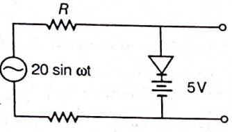
Assuming an ideal diode, draw the output waveform for the circuit given in the figure, explain the waveform.
2.
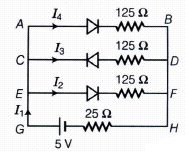
If each diode in figure has a forward bias resistance of \(25\Omega \) and infinite resistance in reverse bias, what will be the values of the currents \(I_{ 1 },I_{ 2 },I_{ 3 } \ and \ I_{ 4 }\) ?
3.
Predict the effect on the electrical properties of a silicon crystal at room temperature, if every millionth silicon atom temperature, if every millionth silicon atom is replaced by an atom of indium. Given, Concentration of silicon atoms = \(5\times { 10 }^{ 28 }{ m }^{ -3 }\) intrinsic carrier concentration = \(1.5\times { 10 }^{ 16 }{ m }^{ -3 }\) He = 0.135 m3/ V-s and Hh = 0.048 m3 / V-s.
4.
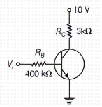
In the circuit shown in figure, when the input voltage of the base resistance is 10 V, VBE is zero and VCE is also zero. Find the values of IB, IC and \(\beta\)
5.
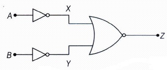
You are given a circuit below. Write its truth table, identify the logic operation carried out by this circuit. Draw the logic symbol of the gate it corresponds.
1.
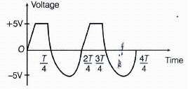
When the input voltage is equal to or less than 5 V, diode will be reverse biased. It will offer high resistance in comparison to resistance (R) in series. now, diode appears in open circuit. The input waveform is then passed to the output terminals. The result with sine wave input is to dip off all positive going portion above 5 V.
If the input voltage is more than +5V, the diode will be conducting as forward biased offering low resistance in comparison to R. But there will be no voltage in output beyond 5 V as the voltage beyond +5V will appear across R.
When input voltage is negative, input voltage becomes more than -5 V (due to 5V battery in reverse bias position), the diode will be reverse biased. It will offer high resistance in comparison to resistance R in series. Now, junction diode appears in open circuit. The input waveform is then passed on to the output terminals. The output waveform is shown here in the figure
2.
Given, forward biased resistance = \(25\Omega \)
Reverse biased resistance = \(\infty \)
As the diode in branch CD is in reverse biased which having resistance infinite.
so \(I_{ 3 }\)= 0
Resistance in branch AB = 25 + 125 = 150\(\Omega \)(say R1)
Resistance in branch EF = 25 + 125 = 150\(\Omega \)(say R2)
AB is parallel to EF.
so, resultant resistance, \(\frac { 1 }{ { R }^{ \prime } } =\frac { 1 }{ { R }_{ 1 } } +\frac { 1 }{ { R }_{ 2 } } =\frac { 1 }{ 150 } +\frac { 1 }{ 150 } =\frac { 2 }{ 150 } \)
\(\Rightarrow { R }^{ \prime }=75\Omega \)
Total resistance, \(R={ R }^{ \prime }+25=75+25=100\Omega \)
Current, \({ I }_{ 1 }=\frac { V }{ R } =\frac { 5 }{ 100 } =0.05A\)
\({ I }_{ 1 }={ I }_{ 4 }+{ I }_{ 2 }+{ I }_{ 3 }\quad [Here,\quad { I }_{ 3 }=0]\)
\(\\ { I }_{ 1 }={ I }_{ 4 }+{ I }_{ 2 }\)
Here, the resistances R1 and R2 are same
\({ I }_{ 4 }={ I }_{ 2 }\)
\(\\ { I }_{ 1 }=2{ I }_{ 2 }\)
\(\\ \Rightarrow { I }_{ 2 }=\frac { { I }_{ 1 } }{ 2 } =\frac { 0.05 }{ 2 } =0.025A\)
\(\\ { I }_{ 4 }=0.025A\)
\(\\ { I }_{ 1 }=0.05A\)
\(\\ { I }_{ 2 }=0.025A\)
\(\\ { I }_{ 3 }=0\)
\(\\ { I }_{ 4 }=0.025A\)
3.
As, Concentration of Si atom \(=5\times { 10 }^{ 28 }\) /m3
The doping of indium is 1 atom 106 atoms of Si. But indium has three valence electrons and each doped indium atom creates one hole in Si crystal. Hence, it acts as an acceptor atom.
Concentration of acceptor atoms,
\({ n }_{ h }=5\times { 10 }^{ 28 }\times { 10 }^{ -6 }=5\times { 10 }^{ 22 }/{ m }^{ 3 }\)
Intrinsic carrier concentration,
\({ n }_{ i }=1.5\times { 10 }^{ 16 }/{ m }^{ 3 }\)
Hole concentration is increased
\(=\frac { { n }_{ h } }{ { n }_{ i } } =\frac { 5\times { 10 }^{ 22 } }{ 1.5\times { 10 }^{ 16 } } =3.33\times { 10 }^{ 6 }\)
New electron concentration,
\({ n }_{ e }=\frac { { n }_{ i }^{ 2 } }{ { n }_{ b } } =\frac { { \left( 1.5\times { 10 }^{ 16 } \right) }^{ 2 } }{ 5\times { 10 }^{ 22 } } =0.45\times { 10 }^{ 10 }/{ m }^{ 3 }\)
Electron concentration has been reduced
\(=\frac { { n }_{ i } }{ { n }_{ e } } =\frac { 1.5\times { 10 }^{ 16 } }{ 0.45\times { 10 }^{ 10 } } =3.33\times { 10 }^{ 6 }\)/m3
This means that the hole concentration has been increased over its intrinsic concentration by the same amount with which the electron concentration has been decreased.
The conductivity of doped silicon is given by
\(\sigma =e\left( { n }_{ e }H_{ e }+{ n }_{ h }H_{ h } \right) \)
\(\\ =\quad 1.6\times { 10 }^{ -19 }\left( 0.45\times { 10 }^{ 10 }\times 0.135+5\times { 10 }^{ 22 }\times 0.048 \right)\)
= 384 S/m
Resistivity, \(\rho =\frac { 1 }{ \sigma } =\frac { 1 }{ 384 } =0.0026\Omega -m\)
Conductivity of pure Si crystal,
\(\sigma ={ en }_{ i }\left( { H }_{ e }+{ H }_{ h } \right) \)
\(\\ =1.6\times { 10 }^{ -19 }\times 1.5\times { 10 }^{ 16 }\left( 0.135+0.048 \right) \)
\(\\ =0.4392\times { 10 }^{ -3 }S/m\)
Resistivity, \(\rho =\frac { 1 }{ \sigma } =\frac { 1 }{ 0.4392\times { 10 }^{ -3 } } =2276.\Omega -m\)
Thus, we see that the conductivity of doped Si becomes much greater than its intrinsic conductivity and the resistivity has become much smaller than the intrinsic resistivity.
4.
Given voltage across RB = 10 V
\(Resistance,{ R }_{ B }=400\kappa \Omega\)
\( { V }_{ BE }=0,{ V }_{ CE }-0 \ { R }_{ C }=3\kappa \Omega\)
\( { I }_{ B }=\frac { Voltage \ across \ { R }_{ B } }{ { R }_{ B } } =\frac { 10 }{ 400\times { 10 }^{ 3 } } \)
\(25\times { 10 }^{ -6 }A=25\mu A\)
\( Voltage \ across{ R }_{ C }=10 \ V\)
\({ I }_{ C }=\frac { Voltage \ across \ { R }_{ c } }{ { R }_{ C } } =\frac { 10 }{ 3\times { 10 }^{ 3 } }\)
\( \beta =\frac { { I }_{ C } }{ { I }_{ B } } =\frac { 3.33\times { 10 }^{ -3 } }{ 25\times { 10 }^{ -6\\ } }\)
\( \beta =1.33\times { 10 }^{ 2 } \)
\(=133\)
5.
Truth table of given circuit is given below:
| A | B | X=\(\overline { A } \) | Y=\(\overline { B } \) | \(Z=\overline { \left( X+Y \right) } =\overline { \overline { A } +\overline { B } } \) |
| 0 | 0 | 1 | 1 | 0 |
| 0 | 1 | 1 | 0 | 0 |
| 1 | 0 | 0 | 1 | 0 |
| 1 | 1 | 0 | 0 | 1 |
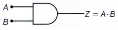
This circuit out the logic operation of AND gate which can be verified also by De-Morgan's theorem
\(Z=\overline { \left( X+Y \right) } =\overline { \overline { A } +\overline { B } } \)
\(Z=\overline { \overline { A } } .\overline { \overline { B } } =A.B\)
This circuit corresponds to AND gate logic symbol is

12th Standard CBSE Syllabus & Materials
12th Standard CBSE
CBSE 12th Computer Science Python Revision Tour I - New Previous year Question Papers Study Material - QB365 Set A
NEW12th Standard CBSE
CBSE 12th Business Studies Planning Important Questions And Answers Study Material - QB365 Set A
NEW12th Standard CBSE
CBSE 12th Business Studies Business Environment Important Questions And Answers Study Material - QB365 Set A
NEW12th Standard CBSE
CBSE 12th Business Studies Principles of Management Important Questions And Answers Study Material - QB365 Set A



NCERT Books

Syllabus

Exam Pattern

Sample Question Papers

Previous year Question Papers

Important Notes

MCQ Practice test

NCERT Exemplers

Case study Questions

Image Based Questions

Passage based Questions

HOT Questions

Value Based Questions

Model Questions Papers
NCERT ( Book Back ) Questions

Assertion and Reason
Important Questions And Answers

CBSE 12th Standard CBSE Subjects
CBSE Standards