
 100% FREE ACCESS
12th Standard CBSE Syllabus & Materials
12th Standard CBSE
CBSE 12th Economics Government Budget and the Economy Previous year Question Papers Study Material - QB365 Set A
NEW12th Standard CBSE
CBSE 12th Computer Science Interface Python with MySQL - New Previous year Question Papers Study Material - QB365 Set A
NEW12th Standard CBSE
CBSE 12th Computer Science Database Concept - New Previous year Question Papers Study Material - QB365 Set A
NEW12th Standard CBSE
CBSE 12th Computer Science Data Communication - New Previous year Question Papers Study Material - QB365 Set A
NEW12th Standard CBSE
CBSE 12th Computer Science Data Structures - New Previous year Question Papers Study Material - QB365 Set A
NEW12th Standard CBSE
CBSE 12th Computer Science Functions - New Previous year Question Papers Study Material - QB365 Set A

Published on: 21/05/2021
QB365 Provides the updated CASE Study Questions for Class 12 , and also provide the detail solution for each and every case study questions . Case study questions are latest updated question pattern from NCERT, QB365 will helps to get more marks in Exams
Download CBSE Class 12th Standard CBSE Physics question papers, sample papers, important questions, and previous year solved papers in PDF format. Get free study materials, NCERT solutions, and exam preparation resources for Class 12th Standard CBSE Physics
Questions + Answers key
Take MCQ Physics Test
1.
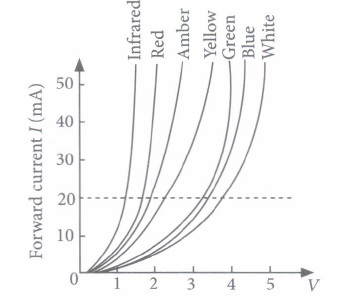
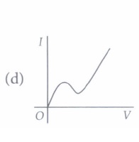
Light emitting diode is a photoelectric device which converts electrical energy into light energy. It is a heavily doped p-n junction diode which under forward biased emits spontaneous radiation. The general shape of the J- V characteristics of an LED is similar to that of a normal p-n junction diode, as shown. The barrier potentials are much higher and slightly different for each colour.
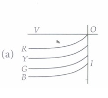
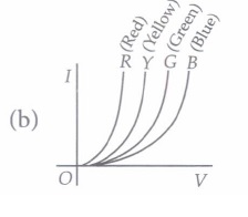
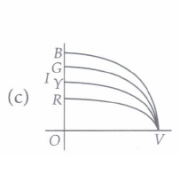
(i) The J- V characteristic of an LED is
 |
 |
 |
 |
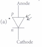
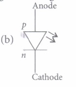
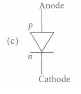
(ii) The schematic symbol of light emitting diode is (LED)
 |
 |
 |
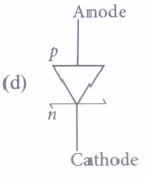 |
(iii) An LED is constructed from a p-n junction based on a certain Ga-As-P semiconducting material whose energy gap is 1.9 eV. Identify the colour of the emitted light.
| (a) Blue | (b) Red | (c) Violet | (d) Green |
(iv) Which one of the following statement is not correct in the case of light emitting diodes?
| (a) It is a heavily doped p-n junction. |
| (b) It emits light only when it is forward biased. |
| (c) It emits light only when it is reverse biased. |
| (d) The energy of the light emitted is less than the energy gap of the semiconductor used |
(v) The energy of radiation emitted by LED is
| (a) greater than the band gap of the semiconductor used |
| (b) always less than the band gap of the semiconductor used |
| (c) always equal to the band gap of the semiconductor used |
| (d) equal to or less than the band gap of the semiconductor used. |
2.
From Bohr's atomic model, we know that the electrons have well defined energy levels in an isolated atom. But due to interatomic interactions in a crystal, the electrons of the outer shells are forced to have energies different from those in isolated atoms. Each energy level splits into a number of energy levels forming a continuous band.The gap between top of valence band and bottom of the conduction band in which no allowed energy levels for electrons can exist is called energy gap.
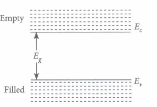
(i) In an insulator energy band gap is
| (a) Eg = 0 | (b) Eg< 3eV | (c) Eg > 3eV | (d) None of the above |
(ii) In a semiconductor, separation between conduction and valence band is of the order of
| (a) 0 eV | (b) 1 eV | (c) 10 eV | (d) 50 eV |
(iii) Based on the band theory of conductors, insulators and semiconductors, the forbidden gap is smallest in
| (a) conductors | (b) insulators | (c) semiconductors | (d) All of these |
(iv) Carbon, silicon and germanium have four valence electrons each. At room temperature which one of the following statements is most appropriate?
| (a) The number of free electrons for conduction is significant only in Si and Ge but small in C. |
| (b) The number of free conduction electrons is significant in C but small in Si and Ge. |
| (c) The number of free conduction electrons is negligibly small in all the three. |
| (d) The number offree electrons for conduction is significant in all the three. |
(v) Solids having highest energy level partially filled with electrons are
| (a) semiconductor | (b) conductor | (c) insulator | (d) none of these |
3.
Rectifier is a device which is used for converting alternating current or voltage into direct current or voltage. Its working is based on the fact that the resistance of p-n junction becomes low when forward biased and becomes high when reverse biased. A half-wave rectifier uses only a single diode while a full wave rectifier uses two diodes as shown in figures (a) and (b) .
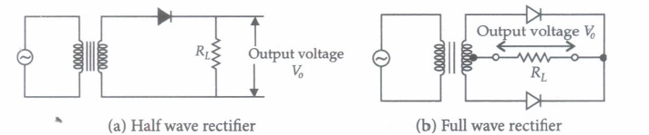
(i) If the rms value of sinusoidal input to a full wave rectifier is \(\frac{V_{0}}{\sqrt{2}}\) then the rms value of the rectifier's output is
| \(\text { (a) } \frac{V_{0}}{\sqrt{2}}\) | \(\text { (b) } \frac{V_{0}^{2}}{\sqrt{2}}\) | \(\text { (c) } \frac{V_{0}^{2}}{2}\) | \(\text { (d) } \sqrt{2} V_{0}^{2}\) |
(ii) In the-diagram, the input ac is actoss the terminals A and C. The output across Band D is
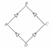
| (a) same as the input | (b) half wave rectified | (c) zero | (d) full wave rectified |
(iii) A bridge rectifier is shown in figure. Alternating input is given across A and C. If output is taken across BD, then it is
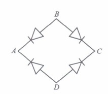
| (a) zero | (b) same as input | (c) half wave rectified | (d) full wave rectified |
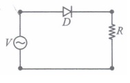
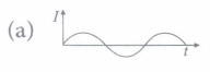
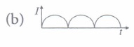
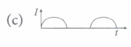
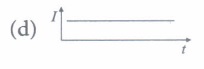
(iv) A p-n junction (D) shown in the figure can act as a rectifier. An alternating current source (V) is connected in the circuit. The current (I) in the resistor(R) can be shown by
 |
 |
 |
 |
(v) With an ac input from 50 Hz power line, the ripple frequency is
| (a) 50 Hz in the dc output of half wave as well as full wave rectifier |
| (b) 100 Hz in the de output of half wave as well as full wave rectifier |
| (c) 50 Hz in the de output of half wave and 100 Hz in dc output offull wave rectifier |
| (d) 100 Hz in the dc output of half wave and 50 Hz in the de output of full wave rectifier |
1.
(i) (b) : The l- V characteristics of an LED is similar to that of a Si junction diode. But the threshold voltages are much higher and slightly different for each colour.
(ii) (b)
(iii) (b) : \(\text { As } E_{g}=\frac{h c}{\lambda} \quad \therefore \lambda=\frac{h c}{E_{g}}\)
Here, Eg = 1.9 eV, he = 1240 eV nm
\(\therefore \quad \lambda=\frac{1240 \mathrm{eVnm}}{1.9 \mathrm{eV}}=652.6 \mathrm{nm}\)
Hence, the emitted light is of red colour.
(iv) (c): A light emitting diode is a heavily doped p-n junction diode which emits light only when it is forward biased.
(v) (d)
2.
(i) (c) :In insulator, energy band gap is > 3 eV
(ii) (b) : In conductor, separation between conduction and valence bands is zero and in insulator, it is greater than 1 eV. Hence in semiconductor the separation between conduction and valence band is 1 eV.
(iii) (a): According to band theory the forbidden gap in conductors Eg = 0, in insulators Eg > 3 eV and in semiconductors Eg < 3 eV.
(iv) (a): The four valence electrons of C, Si and Ge lie respectively in the second, third and fourth orbit.Hence energy required to take out an electron from these atoms (i.e. ionisation energy Eg) will be least for Ge, followed by Si and highest for C. Hence, the number of free electrons for conduction in Ge and Si are significant but negligibly small for C.
(v) (b)
3.
(i) (a) :The rms value of the output voltage at the load resistance \(V_{\mathrm{rms}}=\frac{V_{0}}{\sqrt{2}}\)
(ii) (d)
(iii) (a)
(iv) (c): The given circuit works as a half wave rectifier. In this circuit, we will get current through R when p-n junction is forward biased and no current when p-n junction is reverse biased. Thus the current (I) through resistor (R) will be shown in option (c).
(v) (c)

12th Standard CBSE Syllabus & Materials
12th Standard CBSE
CBSE 12th Computer Science Python Revision Tour I - New Previous year Question Papers Study Material - QB365 Set A
NEW12th Standard CBSE
CBSE 12th Business Studies Planning Important Questions And Answers Study Material - QB365 Set A
NEW12th Standard CBSE
CBSE 12th Business Studies Business Environment Important Questions And Answers Study Material - QB365 Set A
NEW12th Standard CBSE
CBSE 12th Business Studies Principles of Management Important Questions And Answers Study Material - QB365 Set A



NCERT Books

Syllabus

Exam Pattern

Sample Question Papers

Previous year Question Papers

Important Notes

MCQ Practice test

NCERT Exemplers

Case study Questions

Image Based Questions

Passage based Questions

HOT Questions

Value Based Questions

Model Questions Papers
NCERT ( Book Back ) Questions

Assertion and Reason
Important Questions And Answers

CBSE 12th Standard CBSE Subjects
CBSE Standards