
 100% FREE ACCESS
12th Standard Syllabus & Materials
12th Standard
TN 12th Computer Applications மின்னணு தரவு பரிமாற்றம் Sample Question Papers Study Material - QB365 Set A
NEW12th Standard
TN 12th Computer Applications மின் - வணிக பாதுகாப்பு அமைப்புகள் Sample Question Papers Study Material - QB365 Set A
NEW12th Standard
TN 12th Computer Applications மின்னணு செலுத்தல் முறைகள் Sample Question Papers Study Material - QB365 Set A
NEW12th Standard
TN 12th Computer Applications மின் - வணிகம் Sample Question Papers Study Material - QB365 Set A
NEW12th Standard
TN 12th Computer Applications திறந்த மூல கருத்துருக்கள் Sample Question Papers Study Material - QB365 Set A
NEW12th Standard
TN 12th Computer Applications வலையமைப்பு வடமிடல் Sample Question Papers Study Material - QB365 Set A

Published on: 28/11/2025
Download Tamil Nadu 12th Standard Physics question papers, model tests, one-mark questions, important questions, and public exam papers in PDF format. Free study materials and answer keys for TN State Board students.
Questions + Answers key
Take MCQ Physics Test
1.
Elucidate the formation of n-type extrinsic semiconductors.
2.
What is meant by satellite communication? Give its applications.
3.
Explain the working principle of a solar cell. Mention its applications.
4.
State and prove De Morgan’s first and second theorem.
5.
Transistor functions as a switch. Explain.
6.
Describe the function of a transistor as an amplifier with the neat circuit diagram. Sketch the input and output wave forms.
7.
Sketch the static characteristics of a common emitter transistor and bring out the essential features of input and output characteristics.
8.
What is an LED? Give the principle of its operation with a diagram.
9.
Explain the construction and working of a full wave rectifier
10.
Draw the circuit diagram of a half-wave rectifier and explain its working.
11.
Explain the formation of depletion region and barrier potential in PN junction diode.
12.
Give circuit symbol, logical operation, truth table, and Boolean expression of
i) AND gate
ii) OR gate
iii) NOT gate
iv) NAND gate
v) NOR gate and
vi) EX-OR gate.
13.
Fiber optic communication is gaining popularity among the various transmission media -justify.
14.
Explain the ground wave propagation and space wave propagation of electromagnetic waves through space.
15.
Explain the basic elements of communication system with the necessary block diagram.
16.
Explain the ampitude modulation with necessary diagrams.
1.
N-type semiconductor: A n-type semiconductor is obtained by doping a pure Germanium (or Silicon) crystal with a dopant from group V pentavalent elements like Phosphorus, Arsenic, and Antimony. The dopant has five valence electrons while the Germanium atom has four valence electrons.
During the process of doping, a few of the Germanium atoms are replaced by the group V dopants. Four of the five valence electrons of the impurity atom are bound with the 4 valence electrons of the neighbouring replaced Germanium atom. The fifth valence electron of the impurity atom will be loosely attached to the nucleus as it has not formed the covalent bond.
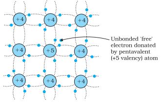
Free electron which is loosely attached to the lattice:
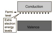
Representation of donor energy level:
The energy level of the loosely attached fifth electron from the dopant is found just below the conduction band edge and is called the donor energy level. At room temperature, these electrons can easily move to the conduction band with the absorption of thermal energy. It is shown in the figure. Besides, an external electric field also can set free the loosely bound electrons and lead to conduction.
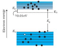
It is important to note that the energy required for an electron to jump from the valence band to the conduction hand in an intrinsic semiconductor is 0.7 eV for Ge and 1.1 eV tor Si, while the energy required to set free Ni a donor electron is only 0.01 eV for Ge and 0.05 eV for Si.
The V group pentavalent impurity atoms donate electrons to the conduction band and are called Onormpunties. Therefore, each impurity atom provides one extra electron to the conduction band in addition to the thermally generated electrons. These thermally generated electrons leave holes in valence band. Hence, the majority carriers of current in an n-type semiconductor are electrons and the minority carriers are holes. Such a semiconductor doped with a pentavalent impurity is called an n-type semiconductor
2.
(i) The satellite communication is a mode of transmission of signal between transmitter and receiver via satellite.
(ii) The message signal from the Earth station is transmitted to the satellite on board via an uplink (frequency band 6 GHz), amplified by a transponder and then retransmitted to another earth station via a downlink (frequency band 4 GHz).
Applications:
Satellites are classified into different types based on their applications.
(i) Weather Satellites:
They are used to monitor the weather and climate of Earth. By measuring cloud mass, these satellites enable us to predict rain and dangerous storms like hurricanes, cyclones etc.
(ii) Communication satellites:
They are used to transmit television, radio, internet signals etc. Multiple satellites are used for long distance communication
(iii) Navigation satellites:
These are employed to determine the geographic location of ships, aircraft or any other object.
3.
A solar cell, also known as photovoltaic cell, works on the principle of photovoltaic effect Accordingly, the p-n junction of the solar cell generates emf when solar radiation falls on it. The construction details and cross-sectional view are shown in Figure.
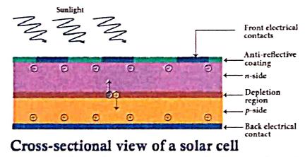
(i) In a solar cell, electron-hole pairs are generated due to the absorption of light near the junction.
(ii) Then the charge carriers are separated due to the electric field of the depletion region.
(iii) Electrons move towards n-type Silicon and holes move towards p-type Silicon layer.
(iv) The electrons reaching the n-side are collected by the front contact and holes reaching p-side are collected by the back electrical contact. Thus a potential difference is developed across solar cell.
(v) When an external load is connected to the solar cell, photocurrent flows through the load.
(vi) Many solar cells are connected together either in series or in parallel combination to form solar panel.
(vii) Many solar panels are connected with each other to form solar arrays.
(viii) For high power applications, solar panels and solar arrays are used.
Applications:
(i) Solar cells are widely used in calculators, watches, toys, portable power supplies, etc.
(ii) Solar cells are used in satellites and space applications.
(iii) Solar panels are used for commercial production of electricity.
4.
First Theorem :
The complement of the sum of two logical inputs is equal to the product of its complements.
\(\overline { A+B } \) = \(\bar { A } .\bar { B } \)
Proof:
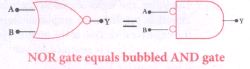
(i) The Boolean equation for NOR gate is Y = \(\overline { A+B } \)
(ii) The Boolean equation for a bubbled AND gate is Y =\(\bar { A } .\bar { B } \)
(iii) Both cases generate same outputs for same inputs. It can be verified using the following truth
| A | B | A+B | \(\overline { A+B } \) | Ā | \(\bar { B } \) | \(\bar { A } .\bar { B } \) |
| 0 | 0 | 0 | 1 | 1 | 1 | 1 |
| 0 | 1 | 1 | 0 | 1 | 0 | 0 |
| 1 | 0 | 1 | 0 | 1 | 0 | 0 |
| 1 | 1 | 1 | 0 | 0 | 0 | 0 |
(i) From the above truth table, we can conclude \(\overline { A+B } \) = \(\bar { A } .\bar { B } \)
(ii) Thus De Morgan's first theorem is proved.
(iii) Hence, a NOR gate is equal to a bubbled AND gate
Second theorem :
The complement of the product of two is equal to the sum of its complements
\(\overline { A.B } \) = \(\bar { A } +\bar { B } \)
Proof:
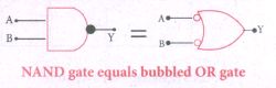
(i) The Boolean equation for NAND gate is Y = \(\overline { A.B } \)
(ii) The Boolean equation for bubbled OR gate is Y = \(\bar { A } +\bar { B } \)
(iii) A and B are the inputs and Y is the output. The above two equations produces the same output for the same inputs. It can be verified by using the truth table.
| A | B | A+B | \(\overline{\mathrm{A}. \mathrm{B}}\) | Ā | \(\bar { B } \) | \(\overline{\mathrm{A}}+\overline{\mathrm{B}}\) |
| 0 | 0 | 0 | 1 | 1 | 1 | 1 |
| 0 | 1 | 0 | 1 | 1 | 0 | 1 |
| 1 | 0 | 0 | 1 | 0 | 1 | 1 |
| 1 | 1 | 1 | 0 | 0 | 0 | 0 |
(i) From the above truth table, we can conclude \(\overline { A.B } \) = \(\bar { A } +\bar { B } \)
(ii) Thus, De Morgan's second therom is proved.
(iii) Hence, a NAND gate is equal to a bubbled OR gate.
5.
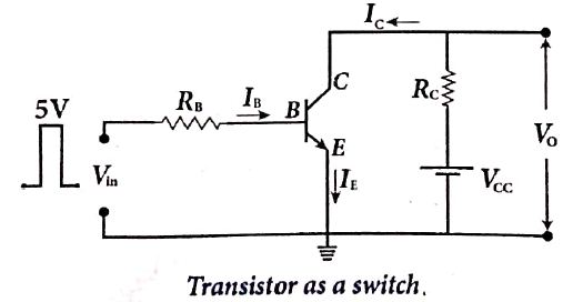
(i) The transistor in saturation region acts as a closed switch while in cut-off region, it acts as an open switch.
(ii) It functions like an electronic switch that helps to turn ON or OFF a given circuit by a small control signal which keeps the transistor either in saturation region or in cut-off region.
When the input is low:
(i) When the input is low (say 0 V), the base current is zero and transistor is not properly forward biased.
(ii) It is in cut off region, As a result, the collector current is zero and correspondingly the voltage drop across RC, also becomes nearly zero, The output voltage is high and Is equal to VCC.
(iii) It means that the no current flows through the transistor and it is said to be switched off. The transistor acts as an open switch.
When the input is high:
(i) When input voltage is increased to a certain high value (say +5 V), the base current (IB) increases and in turn decreases the collector current to its maximum.
(ii) The transistor will move into the saturation region. The increase in collector current (IC). increases the voltage drop across RC, thereby thereby lowering the output voltage, close to zero (since Vo = VCC -ICRC). It means that maximum current flows through the transistor and it is said to be switched on.
(iii)The transistor acts as a closed switch.
6.
Construction:
(a) The amplification of an electrical signal is explained with a single-stage transistor amplifier as shown in figure.
(b) Single stage indicate that the circuit consists of one transistor with the allied components.
.JPG)
(i) An NPN transistor is connected in the common-emitter configuration
(ii) To start with, the Q point or the operating point of the transistor is fixed, so as to get the maximum signal swing at the output (neither towards saturation point nor towards cut-off).
(iii) A load resistance, RC is connected in series with the collector circuit to measure the output voltage.
The resistance R1, R2, and RE, form the biasing and stabilization circuit.
(iv) The capacitor C, allows only the AC signal to pass through.
(v) The emitter by pass capacitor CE provides a low reactance path to the amplified AC signal
(vi) The coupling capacitor CC is used to couple one stage of the amplifier with the next stage, while constructing multistage amplifiers
Vs is the sinusoidal input signal source applied across the base-emitter. The output is taken across the collector-emitter.
Collector current IC = βIB [∵β = IC/IB]
Applying Kirchhoff's voltage law to the output loop, the collector-emitter voltage is given by
VCE = VCC - ICRC
Working of the amplifier :
During the positive half cycle :
(i) Input signal (Vs) increases the forward voltage across the emitter base. As a result, the base current (IB in μA) increases. consequently the collector current (ICin mA) increases β times.
(ii) This increase the voltage drop across RC(ICRC) which in turn decreases the collector-emitter voltage (vCE). Therefore, the input signal in the positive direction produces an amplified signal in the negative direction at the output. Hence the output signal is reversed by 1800 as shown in figure
.JPG)
During the negative half cycle:
(i) Input signal (Vs) decreases the forward voltage across the emitter base. As a result base current (IB in μA) decreases and in tum increases the collector current (IB in μA).
(ii) The increase in collector current (IC) decreases the potential drop across RC and increases the collector - emitter voltage (VCE).
(iii) Thus the input signal in the negative. direction produces an amplified signal in the positive direction at the output.
(iv) Therefore, 180 phase reverse is observed during the negative half cycle of the input signal as well as shown in figure.
7.
.JPG)
The static characteristics of the BJT are
(i) Input characteristics
(ii) Output characteristics
(iii) Transfer characteristics.
(i) Input characteristics:
Input characteristics curves give the relationship between the base current (IB) and base to emitter voltage (vBE) at constant collector to emitter voltage (vCE) and are shown in figure
.JPG)
(i) Initially, the collector to emitter voltage (VCE) is set to a particular value (above 0.7 V to reverse bias the junction).
(ii) Then the base-emitter voltage VBE, is increased in suitable steps and the corresponding base-current IB is recorded.
(iii) A graph is plotted with VBE along the x axis and IB along the Y - axis
(iv) The procedure is repeated for different values of VcE
The following observations are made from the graph :
(i) The Curve looks like the forward characteristics of an ordinary p - n junction diode.
(ii) There exists a threshold voltage (or) knee voltage (Vknee) below which the base current (Ib) is very small. This value is 0.7 V for silicon and 0.3 V for germanium transistors. Beyond the knee voltage, the base current increases with the increase in base-emitter voltage.
(iii) It is also noted the increase in VCE, decreases the IB. This shifts the curve outward.
(iv) This is because the increase in collector-emitter voltage increases the width of the depletion region which in turn, reduces the effective base width and thereby the base current.
Input resistance :
The ratio of the change in base-emitter voltage (∆VBE) to the change in base current (∆LB) at a constant collector-emitter voltage (VCE) is called the input resistance (ri)
\(\mathrm{R}_{\mathrm{i}}=\left[\frac{\Delta \mathrm{V}_{\mathrm{BE}}}{\Delta \mathrm{I}_{\mathrm{B}}}\right]_{\dot{\mathrm{V} C \mathrm{E}}}\)
The input impedance is high for a transistor in common emitter configuration.
Output characteristics :
The output characteristics give the relationship between the collector current (Ic) and the collector -emitter voltage (VCE) at constant input current (IB)
as shown in figure
.JPG)
(i) Initially IB is set to a particular voltage. VCE is increased in suitable steps and IC is recorded
(ii) A graph is plotted with the VCE along the x-axis and IC along the y - axis
(iii) This procedure is repeated for different values IB
The four important regions ln the output characteristics
(i) Saturation region
(ii) Cut-off region
(iii) Active region
(iv) Breakdown region
Output Resistance :
The ratio of the change in the collector emitter voltage (∆VCE) to the corresponding change in the collector current (∆lC) at constant base current (IB) is called output resistance (ro).
\(\mathrm{R}_{\mathrm{o}}=\left[\frac{\Delta \mathrm{V}_{\mathrm{BE}}}{\Delta \mathrm{I}_{\mathrm{C}}}\right]_{\mathrm{l}_{\mathrm{B}}}\)
The output impedance for transistor in common emitter configuration is very low.
8.
LED:
(i) LED is a p-n junction diode that emits visible or invisible light when it is forward biased.
(ii) Since, electrical energy is converted into light energy, this process is also called electroluminescence.
Principle of Operation :
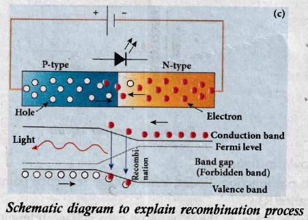
(iii) When the p-n junction is forward biased, the conduction band electrons on the n-side and valence band holes on the p-side diffuse across the junction.
(vi) When they cross the junction, they become excess minority carriers (electrons in p-side and holes in n-side).
(vii) These excess minority carriers recombine with oppositely charged majority carriers in the respective regions, (i.e). the electrons in the conduction band recombine with holes in the valence band.
(viii) During the recombination process, energy is released in the form of light (radiative) or heat (non-radiative). For radiative recombination, a photon of energy h1 is emitted. For non - radiative recombination energy is liberated in the form of heat.
(ix) The colour of the light is determined by the energy bandgap of the material.
(x) Therefore, LEDs are available in a wide range of colours such as blue (SiC), green (AIGaP) and red (GaAsP). Now a days, LED which emits white light (GalnN) is also available.
9.
FuIl wave rectifier :
The positive and negative half cycles of the AC input signal pass through the full wave rectifier circuit and hence it is called the full wave rectifier
Construction:
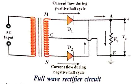
(i) It consists of two p-n junction diodes, a center-tapped transformer, and a load resistor (R1)
(ii) The centre is usually taken as the ground or zero voltage reference point.
(iii) Due to the centre tap transformer, the output voltage rectified by each diode is only one-half of the total secondary voltage.
Working:
During positive half cycle :
(i) When the positive half cycle of the ac input signal passes through the circuit, terminal M is positive, G is at zero potential and N is at negative potential.
(ii) This forward biases diode D1 and reverse biases diode D2.
(iii) Hence, being forward biased, diode D1 conducts and current flows along the path MD1AGC.
During negative half cycle:
(i) When the negative half cycle of the AC input signal passes through the circuit, terminal N becomes positive, C is at zero potential and M is at negative potential.
(ii) This forward biases diode D2 and reverse biases diode D1.
(iii) Hence, being forward biased, diode D2 conducts and current flows along the path ND2BGC.
(iii) During both positive and negative half cycles of the input signal, the current flows through the load in same direction.
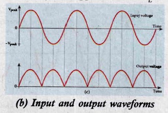
(iv) The output signal corresponding to the input signal is shown in Figure. Though both half cycles of AC input are rectified, the output is still pulsating in nature.
(v) The efficiency (η) of full wave rectifier is twice that of a half wave rectifier and is found to be 81.2 %.
10.
HaIf wave rectifier:
Only one half of the input wave reaches the output. Therefore it is called half wave rectifier.
Construction:
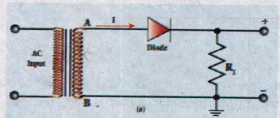
(i) The circuit consists of a transformer, a p-n junction diode and a resistor
(ii) In a half wave rectifier circuit, either a positive half or the negative half of the AC input is passed through by the diode while the other half is blocked
(iii) It acts as a rectifier diode.
.jpg)
(iv) Efficiency (η) is the ratio of the output DC power to the AC input power circuit. supplied to the circuit.
(v) The efficiency (η) of a half wave rectifier is found to be 40.6 %.
.jpg)
11.
i) Formation of depletion layer
(i) A single piece of semiconductor crystal is suitably doped such that its one side is p-type semiconductor and the other side is n-type semiconductor.
(ii) The contact surface between the two sides is called p-n junction. Whenever p-n junction is formed, some of the free electrons diffuse from the n-side to the p-side while the holes from the P-Side to the n-side.
(iii) The diffusion of charge carriers happens due to the fact that the n-side has higher electron concentration and the p-side has higher hole concentration.
(iv) The diffusion of the majority charge carriers across the junction gives rise to an electric current, called diffusion current.
(v) When an electron leaves the n-side, a pentavalent atom in the n-side becomes a positive ion.
(vi) The free electron migrating into p-side recombines with a hole present in a trivalent atom near the junction and the trivalent atom becomes a negative ion. Since such ions are bonded to the neighbouring atoms in the crystal lattice, they are unable to move.
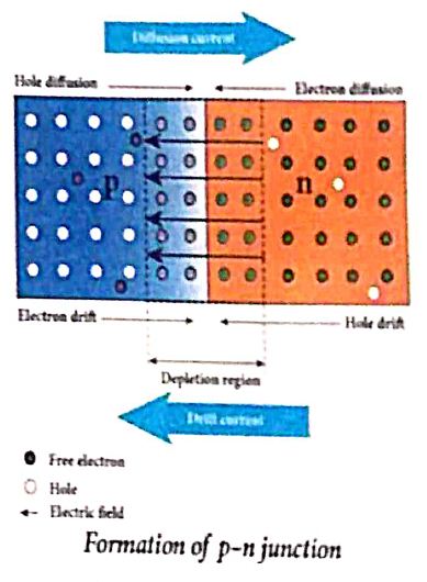
(vii) As the diffusion process continues, a laver of positive ions and a layer of negative ions are created on either side of the junction accordingly.
(viii) The thin region near the junction which is free from charge carriers (free electrons and holes) is called depletion region.
(ix) An electric field is set up between the positively charged layer in the n-side and the negatively charged layer in the p-side in the depletion region.
(x) This electric field makes electrons in the p-side drift into the n-side and the holes in the n-side into the p-side.
(xi) The electric current produced due to the motion of the minority charge carriers by the electric field is known as drift current. The diffusion current and drift current flow in opposite directions.
(xii) Though drift current is less than diffusion current initially, equilibrium is reached between them at a particular time.
(xiii) With each electron (or hole) diffusing across the junction, the strength of the electric field increases thereby increasing the drift current till the two currents become equal
(xiv)Hence at equilibrium, there is no net electric current across the junction. Thus, a p-n junction is formed.
ii) Junction potential or barrier potential
.JPG)
(i) The movement of charge carriers across the junction takes place only to a certain point beyond which the depletion layer acts like a barrier to further diffusion of free charges across the junction.
(ii) This is due to the fact that the immobile ions on both sides establish an electric potential difference across the junction.
(iii) Therefore, an electron trying to diffuse into the interior of the depletion region encounters a wall of negative ions repelling it backwards.
(iv) If the free electron has enough energy, it can break through the wall and enter into the p-region, where it can recombine with a hole and create another negative ion.
(v) The strength of the electric potential difference across the depletion region keeps on increasing with the crossing of each electron until equilibrium is reached, at this point, the internal repulsion of the depletion layer stops further diffusion of free electrons across the junction.
(vi) The difference in potential across the depletion layer is called the barrier potential (Vb).
(vii) At 25°C, this barrier potential is approximately 0.7 V for silicon and 0.3 V for germanium.
12.
i) AND gate
a) Circuit Symbol:
The circuit symbol of a two input AND gate is shown in Figure (a). A and B are inputs and Y is the output. It is a logic gate and hence A, B, and Y can have the value of either 1 or 0
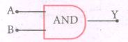
Two input AND gate
| Inputs | outputs | |
| A | B | Y = A + B |
| 0 | 0 | 0 |
| 0 | 1 | 0 |
| 1 | 0 | 0 |
| 1 | 1 | 1 |
Truth table
b) Boolean equation:
Y = A.B
It performs logical multiplication and is different from arithmetic multiplication.
c) Logic operation:
The output of AND gate is high only when all the inputs are high. In the rest of the cases, the output is low. It is represented in the truth table (Figure (b).
ii) OR gate
a) Circuit Symbol:
The circuit symbol of a two input OR gate is shown in Figure (a). A and B are inputs and Y is the output.
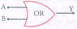
The input OR gate
| Inputs | outputs | |
| A | B | Y = A + B |
| 0 | 0 | 0 |
| 0 | 1 | 1 |
| 1 | 0 | 1 |
| 1 | 1 | 1 |
Truth table
a) Boolean equation:
A + B = Y
It performs logical addition and is different from arithmetic addition.
b) Logic operation:
The output of OR gate is high (logic 1 state) when either of the inputs or both are high. The truth table of OR gate is shown in Figure (a).
iii) NOT gate
a) Circuit Symbol:
The circuit symbol of NOT gate is shown in Figure (a). A and B are inputs and Y is the output.
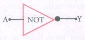
NOT gate
| Inputs | Output |
| A | Y = Ā |
| 0 | 1 |
| 1 | 0 |
Truth table
a) Boolean equation:
Y = Ā
b) Logic operation:
The output is the complement of the input. It is represented with an overbar. It is also called as inverter. The truth table infers that the output Y is I when input A is 0 and vice versa. The truth table of NOT is shown in Figure (b).
iv) NAND gate
a) Circuit Symbol:
The circuit symbol of NAND gate is shown in Figure (a). A and B are inputs and Y is the output.

Two input NAND gate
| Inputs | Output (AND) |
outputs (NAND) |
|
| A | B | Z = A.B | Y = \(\overline { A.B } \) |
| 0 | 0 | 0 | 1 |
| 0 | 1 | 0 | 1 |
| 1 | 0 | 0 | 1 |
| 1 | 1 | 1 | 0 |
Truth table
b) Boolean equation:
Y = \(\overline { A.B } \)
Logic operation:
The output Y equals, the complement of AND operation. The circuit is an AND gate followed by a NOT gate. Therefore, it is summarized as NAND. The output is at logic zero only when all the inputs are high. The rest of the cases, the output is high (Logic I state). The truth table of NAND gate is shown in Figure (b).
v) NOR gate
a) Circuit Symbol:
The circuit symbol of NOR gate is shown in Figure (a). A and B are inputs and Y is the output.

Two input NANS gate
| Inputs | Output (OR) |
outputs (NOR) |
|
| A | B | Z = A + B | Y = \(\overline { A+B } \) |
| 0 | 0 | 0 | 1 |
| 0 | 1 | 1 | 0 |
| 1 | 0 | 1 | 0 |
| 1 | 1 | 1 | 0 |
Truth table
Boolean equation:
Y = \(\overline { A+B } \)
Logic operation:
The output Y equals the complement of OR operation (A OR B). The circuit is an OR gate followed by a NOT gate and is summarized as NOR. The output is high when all the inputs are low. The output is low for all other combinations of inputs. The truth table of NOR gate is shown in Figure (b).
vi) Ex-OR gate
a) Circuit Symbol:
The circuit symbol of Ex-OR gate is shown in Figure (a). A and B are inputs and Y is the output. The Ex-OR operation is denoted as ⊕
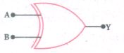
Ex-OR gate
| Inputs | outputs (Ex-OR) |
|
| A | B | Y = A ⊕ B |
| 0 | 0 | 0 |
| 0 | 1 | 1 |
| 1 | 0 | 1 |
| 1 | 1 | 0 |
Truth table
b) Boolean equation
Y = \(A.\overline { B } \) + \(\overline { A }.B \)
Y = A ⊕ B
Logic operation:
The output is high only when either of the two inputs is high. In the case of an Ex-OR gate with more than two inputs, the output will be high when odd number of inputs are high. The truth table of Ex-OR gate is shown in Figure (b).
13.
Fiber optic communication:
(i) The method of transmitting information from one place to another in terms of light pulses through an optical fiber is called fiber optic communication. It works on the principle of total internal reflection.
Applications:
(ii) Optical fiber system has a number of applications namely, international communication, inter-city communication, data links, plant and traffic control and defense applications.
(iii) Fiber cables are very thin and weigh lesser than copper cables.
(iv) This system has much larger band width. This means that its information carrying capacity is larger.
(v) Fiber optic system is immune to electrical interferences.
(vi) Fiber optic cables are cheaper than copper cables.
14.
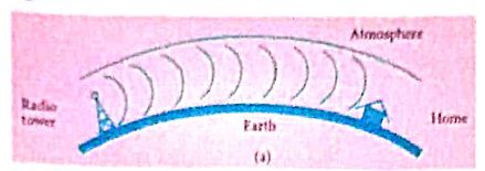
a) Ground wave propagation:
i) If the electromagnetic waves transmitted by the transmitter glide over the surface of the Earth to reach the receiver, then the propagation is called ground wave propagation.
ii) The corresponding waves are called ground waves or surface waves.
iii) Both transmitting and receiving antennas must be close to the Earth's surface.
iv) It is used in local broadcasting, radio navigation, for ship-to-ship, ship-to-shore communication and mobile communication.
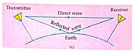
b) Space wave propagation:
i) The process of sending and receiving information signal through space is called space wave communication.
ii) The frequency range for this mode of propagation is above 30 MHz to 400 GHz.
iii) These waves travel in a straight line from the transmitter to the receiver. Hence, it is used for a line of sight (LOS) communication.
iv) Television telecast, satellite communication and RADAR type of communication are based on space wave propagation
v) Range or distance (d) of coverage of propagation depends on height (h) of the antenna given by the equation d = \(\sqrt{2hR}\) where R is radius of the earth, which is R = 6400 km.
15.
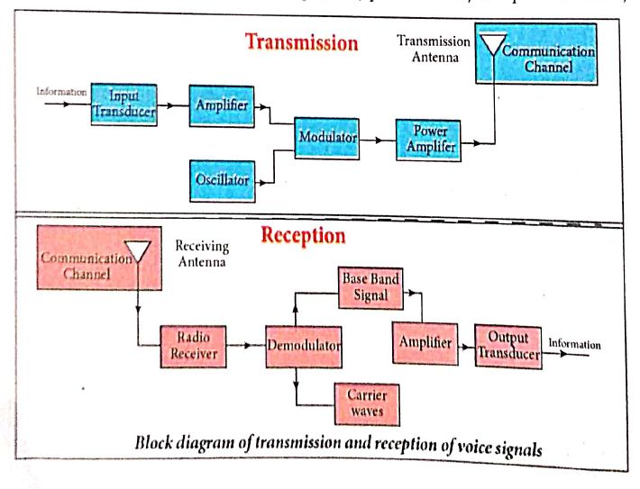
a) Information (Baseband or input signal):
i) Information can be in the form of a sound signal like speech, music, pictures, or computer data which is given as input to the input transducer.
b) Input transducer:
i) It converts the information which is in the form of sound, music, pictures or computer data into corresponding electrical signals.
ii) The electrical equivalent of the original information is called the baseband signal.
iii) The best example is the microphone that converts sound energy into electrical energy.
c) Transmitter
i) It feeds the electrical signal from the transducer to the communication channel
ii) It consists of circuits such as amplifier, oscillator, modulator, and power amplifier.
iii) Amplifier: The transducer output is very weak and is amplified by the amplifier.
iv) Oscillator: It generates high-frequency carrier wave (a sinusoidal wave) for long distance transmission into space. As the energy of a wave is proportional to its frequency, the carrier wave has very high energy.
v) Modulator: It superimposes the baseband signal onto the carrier signal and generates the modulated signal.
vi) Power amplifier: It increases the power level of the electrical signal in order to cover a large distance.
d) Transmitting antenna:
i) It radiates the radio signal into space in all directions.
ii) It travels in the form of electromagnetic waves with the speed of light.
e) Communication channel:
Communication channel is used to carry the electrical signal from transmitter to receiver with less noise or distortion.
Example: Wires, cables, optical fibres in wireline communication and free space in wireless communication.
f) Receiver:
i) The signals that are transmitted through the communication medium are received with the help of a receiving antenna and are fed into the receiver.
ii) The receiver consists of electronic circuits like demodulator, amplifier, detector etc. The demodulator extracts the baseband signal from the carrier signal.
iii) Then the baseband signal is detected and amplified using amplifiers.
iv) Finally, it is fed to the output transducer.
g) Repeaters:
i) Repeaters are used to increase the range or distance through which the signals are sent.
ii) It is a combination of transmitter and receiver.
iii) The signals are received, amplified, and retransmitted with a carrier signal of different frequency to the destination.
iv) The best example is the communication satellite in space
h) Output transducer:
i) It converts the electrical signal back to its original form such as sound, music, pictures or data.
ii) Examples of output transducers are loudspeakers, picture tubes, computer monitor, etc
16.
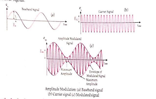
(i) If the amplitude of the carrier signal is modified according to the instantaneous amplitude of the baseband signal, then it is called amplitude modulation Here the frequency and the phase, of the carrier signal remain constant. Amplitude modulation is used in radio and TV broadcasting.
(ii) The signal shown in Figure (a) is the baseband signal that carries information. Figure(b) show the high-frequency carrier signal and Figure (c) gives amplitude modulated signal. We can see that amplitude of the carrier wave is modified in proportion to the amplitude or the baseband signal.

12th Standard Syllabus & Materials
12th Standard
TN 12th Computer Applications களப்பெயர் முறைமை (DNS) Sample Question Papers Study Material - QB365 Set A
NEW12th Standard
TN 12th Computer Applications வலையமைப்பு எடுத்துக்காட்டுகள் மற்றும் நெறிமுறைகள் Sample Question Papers Study Material - QB365 Set A
NEW12th Standard
TN 12th Computer Applications கணினி வலையமைப்பு ஓர் அறிமுகம் Sample Question Papers Study Material - QB365 Set A
NEW12th Standard
TN 12th Computer Applications PHP-உடன் MySQL-ஐ இணைத்தல் Sample Question Papers Study Material - QB365 Set A



Tamilnadu Stateboard 12th Standard Subjects

Maths

Chemistry
Physics

Biology

Computer Science

Business Maths and Statistics

Economics

Commerce

Accountancy

History

Computer Applications
Biology
Computer Technology
Computer Applications
Computer Science
Business Maths and Statistics
Commerce
Economics
Maths
Chemistry
Physics
Computer Technology
History
Accountancy

Tamil

English

French
Tamilnadu Stateboard Standards


