
 100% FREE ACCESS
12th Standard Syllabus & Materials
12th Standard
TN 12th Computer Applications மின்னணு தரவு பரிமாற்றம் Sample Question Papers Study Material - QB365 Set A
NEW12th Standard
TN 12th Computer Applications மின் - வணிக பாதுகாப்பு அமைப்புகள் Sample Question Papers Study Material - QB365 Set A
NEW12th Standard
TN 12th Computer Applications மின்னணு செலுத்தல் முறைகள் Sample Question Papers Study Material - QB365 Set A
NEW12th Standard
TN 12th Computer Applications மின் - வணிகம் Sample Question Papers Study Material - QB365 Set A
NEW12th Standard
TN 12th Computer Applications திறந்த மூல கருத்துருக்கள் Sample Question Papers Study Material - QB365 Set A
NEW12th Standard
TN 12th Computer Applications வலையமைப்பு வடமிடல் Sample Question Papers Study Material - QB365 Set A

Published on: 28/11/2025
Download Tamil Nadu 12th Standard Physics question papers, model tests, one-mark questions, important questions, and public exam papers in PDF format. Free study materials and answer keys for TN State Board students.
Questions + Answers key
Take MCQ Physics Test
1.
State and prove De Morgan’s first and second theorem.
2.
Transistor functions as a switch. Explain.
3.
Describe the function of a transistor as an amplifier with the neat circuit diagram. Sketch the input and output wave forms.
4.
Explain the construction and working of a full wave rectifier
5.
Draw the circuit diagram of a half-wave rectifier and explain its working.
6.
Explain the formation of depletion region and barrier potential in PN junction diode.
7.
Explain the ampitude modulation with necessary diagrams.
8.
List out the advantages and limitations of frequency modulation.
9.
Write a note on photodiode.
1.
First Theorem :
The complement of the sum of two logical inputs is equal to the product of its complements.
\(\overline { A+B } \) = \(\bar { A } .\bar { B } \)
Proof:
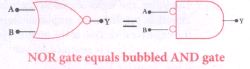
(i) The Boolean equation for NOR gate is Y = \(\overline { A+B } \)
(ii) The Boolean equation for a bubbled AND gate is Y =\(\bar { A } .\bar { B } \)
(iii) Both cases generate same outputs for same inputs. It can be verified using the following truth
| A | B | A+B | \(\overline { A+B } \) | Ā | \(\bar { B } \) | \(\bar { A } .\bar { B } \) |
| 0 | 0 | 0 | 1 | 1 | 1 | 1 |
| 0 | 1 | 1 | 0 | 1 | 0 | 0 |
| 1 | 0 | 1 | 0 | 1 | 0 | 0 |
| 1 | 1 | 1 | 0 | 0 | 0 | 0 |
(i) From the above truth table, we can conclude \(\overline { A+B } \) = \(\bar { A } .\bar { B } \)
(ii) Thus De Morgan's first theorem is proved.
(iii) Hence, a NOR gate is equal to a bubbled AND gate
Second theorem :
The complement of the product of two is equal to the sum of its complements
\(\overline { A.B } \) = \(\bar { A } +\bar { B } \)
Proof:
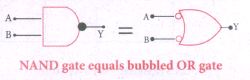
(i) The Boolean equation for NAND gate is Y = \(\overline { A.B } \)
(ii) The Boolean equation for bubbled OR gate is Y = \(\bar { A } +\bar { B } \)
(iii) A and B are the inputs and Y is the output. The above two equations produces the same output for the same inputs. It can be verified by using the truth table.
| A | B | A+B | \(\overline{\mathrm{A}. \mathrm{B}}\) | Ā | \(\bar { B } \) | \(\overline{\mathrm{A}}+\overline{\mathrm{B}}\) |
| 0 | 0 | 0 | 1 | 1 | 1 | 1 |
| 0 | 1 | 0 | 1 | 1 | 0 | 1 |
| 1 | 0 | 0 | 1 | 0 | 1 | 1 |
| 1 | 1 | 1 | 0 | 0 | 0 | 0 |
(i) From the above truth table, we can conclude \(\overline { A.B } \) = \(\bar { A } +\bar { B } \)
(ii) Thus, De Morgan's second therom is proved.
(iii) Hence, a NAND gate is equal to a bubbled OR gate.
2.
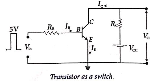
(i) The transistor in saturation region acts as a closed switch while in cut-off region, it acts as an open switch.
(ii) It functions like an electronic switch that helps to turn ON or OFF a given circuit by a small control signal which keeps the transistor either in saturation region or in cut-off region.
When the input is low:
(i) When the input is low (say 0 V), the base current is zero and transistor is not properly forward biased.
(ii) It is in cut off region, As a result, the collector current is zero and correspondingly the voltage drop across RC, also becomes nearly zero, The output voltage is high and Is equal to VCC.
(iii) It means that the no current flows through the transistor and it is said to be switched off. The transistor acts as an open switch.
When the input is high:
(i) When input voltage is increased to a certain high value (say +5 V), the base current (IB) increases and in turn decreases the collector current to its maximum.
(ii) The transistor will move into the saturation region. The increase in collector current (IC). increases the voltage drop across RC, thereby thereby lowering the output voltage, close to zero (since Vo = VCC -ICRC). It means that maximum current flows through the transistor and it is said to be switched on.
(iii)The transistor acts as a closed switch.
3.
Construction:
(a) The amplification of an electrical signal is explained with a single-stage transistor amplifier as shown in figure.
(b) Single stage indicate that the circuit consists of one transistor with the allied components.
.JPG)
(i) An NPN transistor is connected in the common-emitter configuration
(ii) To start with, the Q point or the operating point of the transistor is fixed, so as to get the maximum signal swing at the output (neither towards saturation point nor towards cut-off).
(iii) A load resistance, RC is connected in series with the collector circuit to measure the output voltage.
The resistance R1, R2, and RE, form the biasing and stabilization circuit.
(iv) The capacitor C, allows only the AC signal to pass through.
(v) The emitter by pass capacitor CE provides a low reactance path to the amplified AC signal
(vi) The coupling capacitor CC is used to couple one stage of the amplifier with the next stage, while constructing multistage amplifiers
Vs is the sinusoidal input signal source applied across the base-emitter. The output is taken across the collector-emitter.
Collector current IC = βIB [∵β = IC/IB]
Applying Kirchhoff's voltage law to the output loop, the collector-emitter voltage is given by
VCE = VCC - ICRC
Working of the amplifier :
During the positive half cycle :
(i) Input signal (Vs) increases the forward voltage across the emitter base. As a result, the base current (IB in μA) increases. consequently the collector current (ICin mA) increases β times.
(ii) This increase the voltage drop across RC(ICRC) which in turn decreases the collector-emitter voltage (vCE). Therefore, the input signal in the positive direction produces an amplified signal in the negative direction at the output. Hence the output signal is reversed by 1800 as shown in figure
.JPG)
During the negative half cycle:
(i) Input signal (Vs) decreases the forward voltage across the emitter base. As a result base current (IB in μA) decreases and in tum increases the collector current (IB in μA).
(ii) The increase in collector current (IC) decreases the potential drop across RC and increases the collector - emitter voltage (VCE).
(iii) Thus the input signal in the negative. direction produces an amplified signal in the positive direction at the output.
(iv) Therefore, 180 phase reverse is observed during the negative half cycle of the input signal as well as shown in figure.
4.
FuIl wave rectifier :
The positive and negative half cycles of the AC input signal pass through the full wave rectifier circuit and hence it is called the full wave rectifier
Construction:
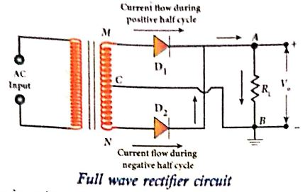
(i) It consists of two p-n junction diodes, a center-tapped transformer, and a load resistor (R1)
(ii) The centre is usually taken as the ground or zero voltage reference point.
(iii) Due to the centre tap transformer, the output voltage rectified by each diode is only one-half of the total secondary voltage.
Working:
During positive half cycle :
(i) When the positive half cycle of the ac input signal passes through the circuit, terminal M is positive, G is at zero potential and N is at negative potential.
(ii) This forward biases diode D1 and reverse biases diode D2.
(iii) Hence, being forward biased, diode D1 conducts and current flows along the path MD1AGC.
During negative half cycle:
(i) When the negative half cycle of the AC input signal passes through the circuit, terminal N becomes positive, C is at zero potential and M is at negative potential.
(ii) This forward biases diode D2 and reverse biases diode D1.
(iii) Hence, being forward biased, diode D2 conducts and current flows along the path ND2BGC.
(iii) During both positive and negative half cycles of the input signal, the current flows through the load in same direction.
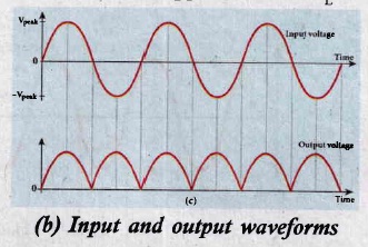
(iv) The output signal corresponding to the input signal is shown in Figure. Though both half cycles of AC input are rectified, the output is still pulsating in nature.
(v) The efficiency (η) of full wave rectifier is twice that of a half wave rectifier and is found to be 81.2 %.
5.
HaIf wave rectifier:
Only one half of the input wave reaches the output. Therefore it is called half wave rectifier.
Construction:
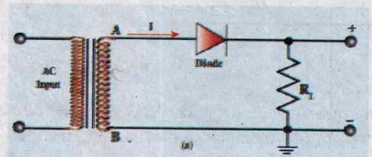
(i) The circuit consists of a transformer, a p-n junction diode and a resistor
(ii) In a half wave rectifier circuit, either a positive half or the negative half of the AC input is passed through by the diode while the other half is blocked
(iii) It acts as a rectifier diode.
.jpg)
(iv) Efficiency (η) is the ratio of the output DC power to the AC input power circuit. supplied to the circuit.
(v) The efficiency (η) of a half wave rectifier is found to be 40.6 %.
.jpg)
6.
i) Formation of depletion layer
(i) A single piece of semiconductor crystal is suitably doped such that its one side is p-type semiconductor and the other side is n-type semiconductor.
(ii) The contact surface between the two sides is called p-n junction. Whenever p-n junction is formed, some of the free electrons diffuse from the n-side to the p-side while the holes from the P-Side to the n-side.
(iii) The diffusion of charge carriers happens due to the fact that the n-side has higher electron concentration and the p-side has higher hole concentration.
(iv) The diffusion of the majority charge carriers across the junction gives rise to an electric current, called diffusion current.
(v) When an electron leaves the n-side, a pentavalent atom in the n-side becomes a positive ion.
(vi) The free electron migrating into p-side recombines with a hole present in a trivalent atom near the junction and the trivalent atom becomes a negative ion. Since such ions are bonded to the neighbouring atoms in the crystal lattice, they are unable to move.
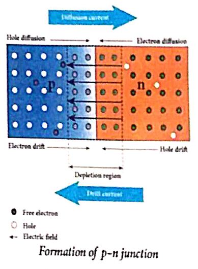
(vii) As the diffusion process continues, a laver of positive ions and a layer of negative ions are created on either side of the junction accordingly.
(viii) The thin region near the junction which is free from charge carriers (free electrons and holes) is called depletion region.
(ix) An electric field is set up between the positively charged layer in the n-side and the negatively charged layer in the p-side in the depletion region.
(x) This electric field makes electrons in the p-side drift into the n-side and the holes in the n-side into the p-side.
(xi) The electric current produced due to the motion of the minority charge carriers by the electric field is known as drift current. The diffusion current and drift current flow in opposite directions.
(xii) Though drift current is less than diffusion current initially, equilibrium is reached between them at a particular time.
(xiii) With each electron (or hole) diffusing across the junction, the strength of the electric field increases thereby increasing the drift current till the two currents become equal
(xiv)Hence at equilibrium, there is no net electric current across the junction. Thus, a p-n junction is formed.
ii) Junction potential or barrier potential
.JPG)
(i) The movement of charge carriers across the junction takes place only to a certain point beyond which the depletion layer acts like a barrier to further diffusion of free charges across the junction.
(ii) This is due to the fact that the immobile ions on both sides establish an electric potential difference across the junction.
(iii) Therefore, an electron trying to diffuse into the interior of the depletion region encounters a wall of negative ions repelling it backwards.
(iv) If the free electron has enough energy, it can break through the wall and enter into the p-region, where it can recombine with a hole and create another negative ion.
(v) The strength of the electric potential difference across the depletion region keeps on increasing with the crossing of each electron until equilibrium is reached, at this point, the internal repulsion of the depletion layer stops further diffusion of free electrons across the junction.
(vi) The difference in potential across the depletion layer is called the barrier potential (Vb).
(vii) At 25°C, this barrier potential is approximately 0.7 V for silicon and 0.3 V for germanium.
7.
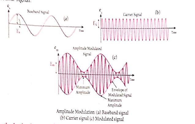
(i) If the amplitude of the carrier signal is modified according to the instantaneous amplitude of the baseband signal, then it is called amplitude modulation Here the frequency and the phase, of the carrier signal remain constant. Amplitude modulation is used in radio and TV broadcasting.
(ii) The signal shown in Figure (a) is the baseband signal that carries information. Figure(b) show the high-frequency carrier signal and Figure (c) gives amplitude modulated signal. We can see that amplitude of the carrier wave is modified in proportion to the amplitude or the baseband signal.
8.
Advantages of FM:
i) In FM, there is a large decrease in noise. This leads to an increase in signal-noise ratio.
ii) The operating range is quite large.
iii) The transmission efficiency is very high as all the transmitted power is useful
iv) FM Bandwidth covers the entire frequency range which humans can hear. Due to this, FM radio has better quality compared to AM radio.
Limitations of FM:
i) FM requires a much wider channel.
ii) FM transmitters and receivers are more complex and costly.
iii) In FM reception, less area is covered compared to AM.
9.
Photo diode:
A p -n junction diode which converts an optical signal into electrical current is known as photodiode.
(i) The operation of photodiode is exactly inverse to that of an LED. Photodiode works in reverse bias condition.
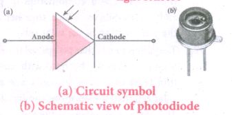
(ii) The direction of arrows indicates that the light is incident on the photo diode.
(iii) The device consists of a p-n junction semiconductor made of photosensitive material kept safely inside a plastic case as shown in fig.
(iv) It has a small transparent window that allows light to be incident on the p-n junction.
(v) Photodiodes car generate current when the p - n junction is exposed to light and hence are called as light sensors.
(vi) When a photon of sufficient energy (hv) strikes the depletion region of the diode, some of the valence band electron are elevated into conduction band, in turn holes are developed in the valence band. This creates electron-hole pairs. The amount of electron - hole pairs generated depends on the intensity of light incident on the p - n junction.
(vii) These electron and holes are swept across the p-n junction by the electric field created by reverse voltage before recombination takes place. Thus, holes move towards the n - side and electrons towards the P - side - when the external circuit is made, the electrons flow through the external circuit and constitute the photo current.
(viii) When the incident light is zero, there exists a reverse current which is negligible. This reverse current in the absence of any. incident light is called dark current and is. due to the thermally generated minority carriers.

12th Standard Syllabus & Materials
12th Standard
TN 12th Computer Applications களப்பெயர் முறைமை (DNS) Sample Question Papers Study Material - QB365 Set A
NEW12th Standard
TN 12th Computer Applications வலையமைப்பு எடுத்துக்காட்டுகள் மற்றும் நெறிமுறைகள் Sample Question Papers Study Material - QB365 Set A
NEW12th Standard
TN 12th Computer Applications கணினி வலையமைப்பு ஓர் அறிமுகம் Sample Question Papers Study Material - QB365 Set A
NEW12th Standard
TN 12th Computer Applications PHP-உடன் MySQL-ஐ இணைத்தல் Sample Question Papers Study Material - QB365 Set A



Tamilnadu Stateboard 12th Standard Subjects

Maths

Chemistry
Physics

Biology

Computer Science

Business Maths and Statistics

Economics

Commerce

Accountancy

History

Computer Applications
Biology
Computer Technology
Computer Applications
Computer Science
Business Maths and Statistics
Commerce
Economics
Maths
Chemistry
Physics
Computer Technology
History
Accountancy

Tamil

English

French
Tamilnadu Stateboard Standards


