
 100% FREE ACCESS
12th Standard Syllabus & Materials
12th Standard
TN 12th Maths Applications of Matrices and Determinants Sample Question Papers Study Material - QB365 Set A
NEW12th Standard
TN 12th Computer Applications மின்னணு தரவு பரிமாற்றம் Sample Question Papers Study Material - QB365 Set A
NEW12th Standard
TN 12th Computer Applications மின் - வணிக பாதுகாப்பு அமைப்புகள் Sample Question Papers Study Material - QB365 Set A
NEW12th Standard
TN 12th Computer Applications மின்னணு செலுத்தல் முறைகள் Sample Question Papers Study Material - QB365 Set A
NEW12th Standard
TN 12th Computer Applications மின் - வணிகம் Sample Question Papers Study Material - QB365 Set A
NEW12th Standard
TN 12th Computer Applications திறந்த மூல கருத்துருக்கள் Sample Question Papers Study Material - QB365 Set A

Published on: 22/08/2026
Download Tamil Nadu 12th Standard Physics question papers, model tests, one-mark questions, important questions, and public exam papers in PDF format. Free study materials and answer keys for TN State Board students.
Questions + Answers key
Take MCQ Physics Test
1.
For a transistor \(\frac{I_C}{I_E}\) = 0.96, then CE current gain is ______________.
12
6
24
48
2.
The frequency range of 3 MHz to 30 MHz is used for ______.
Ground wave propagation
Space wave propagation
Sky wave propagation
Satellite communication
3.
The output of the following circuit is 1 when the input ABC is______.
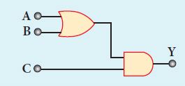
101
100
110
010
4.
The given electrical network is equivalent to ______.

AND gate
OR gate
NOR gate
NOT gate
5.
The electrical series circuit in digital form is
AND
OR
NOR
NAND
6.
7.
The light emitted in an LED is due to ______.
Recombination of charge carriers
Reflection of light due to lens action
Amplification of light falling at the junction
Large current capacity
8.
The principle based on which a solar cell operates is______.
Diffusion
Recombination
Photovoltaic action
Carrier flow
9.
If a positive half-wave rectified voltage is fed to a load resistor, for which part of a cycle there will be current flow through the load?
00–900
900–1800
00–1800
00–3600
10.
The barrier potential of a silicon diode is approximately, ______.
0.7 V
0.3 V
2.0 V
2.2 V
11.
Elucidate the formation of n-type extrinsic semiconductors.
12.
State and prove De Morgan’s first and second theorem.
13.
Explain the construction and working of a full wave rectifier
14.
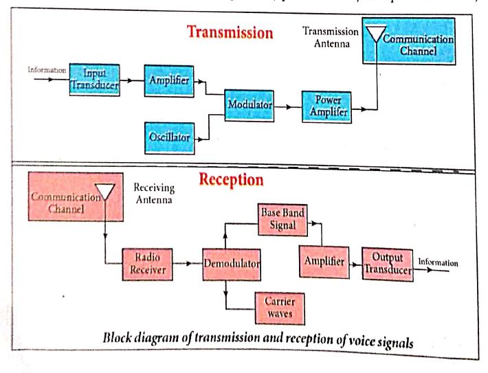
Explain the basic elements of communication system with the necessary block diagram.
15.
Explain the ampitude modulation with necessary diagrams.
16.
Prove the following Boolean expressions using the laws and theorems of Boolean algebra.
(i) \((A+B)(A+\bar{B})=A\)
(ii) \(A(\bar{A}+B)=A B\)
(iii) (A + B) (A + C) = A + BC
17.
Why are NOR and NAND gates called universal gates?
18.
Give the Barkhausen conditions for sustained oscillations.
19.
What is rectification?
20.
A diode is called as a unidirectional device. Explain.
21.
What do you mean by doping?
22.
23.
24.
Write the output (Y) Boolean expression for the following circuit with inputs A, B and C.
.jpg)
25.
Simplify the Boolean identify
AC + ABC = AC
26.
List out the advantages and limitations of frequency modulation.
27.
What are the application of satellite communication?
28.
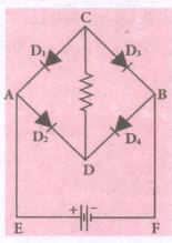
Four silicon diodes and a 10 Ω resistor are connected as shown in figure below. Each diode has a resistance of 1Ω. Find the current flows through the 10Ω resistor.
1.
\(\begin{array}{l} \beta=\frac{a}{1-\alpha} \\ \beta=\frac{0.96}{1-0.96}=24 \end{array}\)
2.
Ground wave propagation: frequency less than 2 MHz
Sky wave propagation: 3 to 30 MHz
Space wave propagation: Above 30 MHz to 400 GHz
Satellite communication: uplink communication 6 GHz band downlink communication 4 GHz band
3.
A = 1, B = 0, C = 1
y = A + B, y = (A + B).C
y = (1 + 0).1 ⇒ y = 1
4.
\(Y_1=\overline{A+B}, y_2=\overline{A+B}=A+B, y=\overline{A+B}\)
5.
(a)
AND
6.
(d)
7.
(a)
Recombination of charge carriers
8.
(c)
Photovoltaic action
9.
(c)
00–1800
10.
(a)
0.7 V
11.
N-type semiconductor: A n-type semiconductor is obtained by doping a pure Germanium (or Silicon) crystal with a dopant from group V pentavalent elements like Phosphorus, Arsenic, and Antimony. The dopant has five valence electrons while the Germanium atom has four valence electrons.
During the process of doping, a few of the Germanium atoms are replaced by the group V dopants. Four of the five valence electrons of the impurity atom are bound with the 4 valence electrons of the neighbouring replaced Germanium atom. The fifth valence electron of the impurity atom will be loosely attached to the nucleus as it has not formed the covalent bond.
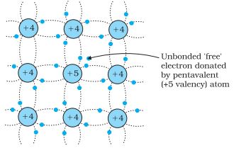
Free electron which is loosely attached to the lattice:
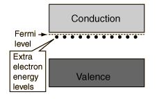
Representation of donor energy level:
The energy level of the loosely attached fifth electron from the dopant is found just below the conduction band edge and is called the donor energy level. At room temperature, these electrons can easily move to the conduction band with the absorption of thermal energy. It is shown in the figure. Besides, an external electric field also can set free the loosely bound electrons and lead to conduction.
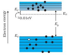
It is important to note that the energy required for an electron to jump from the valence band to the conduction hand in an intrinsic semiconductor is 0.7 eV for Ge and 1.1 eV tor Si, while the energy required to set free Ni a donor electron is only 0.01 eV for Ge and 0.05 eV for Si.
The V group pentavalent impurity atoms donate electrons to the conduction band and are called Onormpunties. Therefore, each impurity atom provides one extra electron to the conduction band in addition to the thermally generated electrons. These thermally generated electrons leave holes in valence band. Hence, the majority carriers of current in an n-type semiconductor are electrons and the minority carriers are holes. Such a semiconductor doped with a pentavalent impurity is called an n-type semiconductor
12.
First Theorem :
The complement of the sum of two logical inputs is equal to the product of its complements.
\(\overline { A+B } \) = \(\bar { A } .\bar { B } \)
Proof:
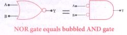
(i) The Boolean equation for NOR gate is Y = \(\overline { A+B } \)
(ii) The Boolean equation for a bubbled AND gate is Y =\(\bar { A } .\bar { B } \)
(iii) Both cases generate same outputs for same inputs. It can be verified using the following truth
| A | B | A+B | \(\overline { A+B } \) | Ā | \(\bar { B } \) | \(\bar { A } .\bar { B } \) |
| 0 | 0 | 0 | 1 | 1 | 1 | 1 |
| 0 | 1 | 1 | 0 | 1 | 0 | 0 |
| 1 | 0 | 1 | 0 | 1 | 0 | 0 |
| 1 | 1 | 1 | 0 | 0 | 0 | 0 |
(i) From the above truth table, we can conclude \(\overline { A+B } \) = \(\bar { A } .\bar { B } \)
(ii) Thus De Morgan's first theorem is proved.
(iii) Hence, a NOR gate is equal to a bubbled AND gate
Second theorem :
The complement of the product of two is equal to the sum of its complements
\(\overline { A.B } \) = \(\bar { A } +\bar { B } \)
Proof:
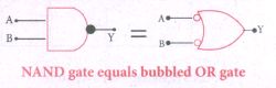
(i) The Boolean equation for NAND gate is Y = \(\overline { A.B } \)
(ii) The Boolean equation for bubbled OR gate is Y = \(\bar { A } +\bar { B } \)
(iii) A and B are the inputs and Y is the output. The above two equations produces the same output for the same inputs. It can be verified by using the truth table.
| A | B | A+B | \(\overline{\mathrm{A}. \mathrm{B}}\) | Ā | \(\bar { B } \) | \(\overline{\mathrm{A}}+\overline{\mathrm{B}}\) |
| 0 | 0 | 0 | 1 | 1 | 1 | 1 |
| 0 | 1 | 0 | 1 | 1 | 0 | 1 |
| 1 | 0 | 0 | 1 | 0 | 1 | 1 |
| 1 | 1 | 1 | 0 | 0 | 0 | 0 |
(i) From the above truth table, we can conclude \(\overline { A.B } \) = \(\bar { A } +\bar { B } \)
(ii) Thus, De Morgan's second therom is proved.
(iii) Hence, a NAND gate is equal to a bubbled OR gate.
13.
FuIl wave rectifier :
The positive and negative half cycles of the AC input signal pass through the full wave rectifier circuit and hence it is called the full wave rectifier
Construction:
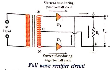
(i) It consists of two p-n junction diodes, a center-tapped transformer, and a load resistor (R1)
(ii) The centre is usually taken as the ground or zero voltage reference point.
(iii) Due to the centre tap transformer, the output voltage rectified by each diode is only one-half of the total secondary voltage.
Working:
During positive half cycle :
(i) When the positive half cycle of the ac input signal passes through the circuit, terminal M is positive, G is at zero potential and N is at negative potential.
(ii) This forward biases diode D1 and reverse biases diode D2.
(iii) Hence, being forward biased, diode D1 conducts and current flows along the path MD1AGC.
During negative half cycle:
(i) When the negative half cycle of the AC input signal passes through the circuit, terminal N becomes positive, C is at zero potential and M is at negative potential.
(ii) This forward biases diode D2 and reverse biases diode D1.
(iii) Hence, being forward biased, diode D2 conducts and current flows along the path ND2BGC.
(iii) During both positive and negative half cycles of the input signal, the current flows through the load in same direction.
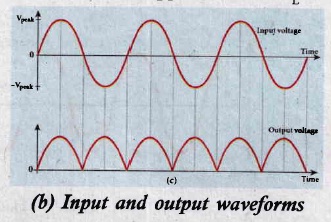
(iv) The output signal corresponding to the input signal is shown in Figure. Though both half cycles of AC input are rectified, the output is still pulsating in nature.
(v) The efficiency (η) of full wave rectifier is twice that of a half wave rectifier and is found to be 81.2 %.
14.
a) Information (Baseband or input signal):
i) Information can be in the form of a sound signal like speech, music, pictures, or computer data which is given as input to the input transducer.
b) Input transducer:
i) It converts the information which is in the form of sound, music, pictures or computer data into corresponding electrical signals.
ii) The electrical equivalent of the original information is called the baseband signal.
iii) The best example is the microphone that converts sound energy into electrical energy.
c) Transmitter
i) It feeds the electrical signal from the transducer to the communication channel
ii) It consists of circuits such as amplifier, oscillator, modulator, and power amplifier.
iii) Amplifier: The transducer output is very weak and is amplified by the amplifier.
iv) Oscillator: It generates high-frequency carrier wave (a sinusoidal wave) for long distance transmission into space. As the energy of a wave is proportional to its frequency, the carrier wave has very high energy.
v) Modulator: It superimposes the baseband signal onto the carrier signal and generates the modulated signal.
vi) Power amplifier: It increases the power level of the electrical signal in order to cover a large distance.
d) Transmitting antenna:
i) It radiates the radio signal into space in all directions.
ii) It travels in the form of electromagnetic waves with the speed of light.
e) Communication channel:
Communication channel is used to carry the electrical signal from transmitter to receiver with less noise or distortion.
Example: Wires, cables, optical fibres in wireline communication and free space in wireless communication.
f) Receiver:
i) The signals that are transmitted through the communication medium are received with the help of a receiving antenna and are fed into the receiver.
ii) The receiver consists of electronic circuits like demodulator, amplifier, detector etc. The demodulator extracts the baseband signal from the carrier signal.
iii) Then the baseband signal is detected and amplified using amplifiers.
iv) Finally, it is fed to the output transducer.
g) Repeaters:
i) Repeaters are used to increase the range or distance through which the signals are sent.
ii) It is a combination of transmitter and receiver.
iii) The signals are received, amplified, and retransmitted with a carrier signal of different frequency to the destination.
iv) The best example is the communication satellite in space
h) Output transducer:
i) It converts the electrical signal back to its original form such as sound, music, pictures or data.
ii) Examples of output transducers are loudspeakers, picture tubes, computer monitor, etc
15.
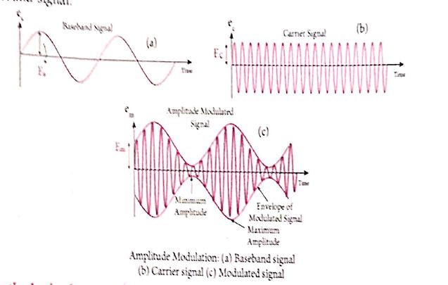
(i) If the amplitude of the carrier signal is modified according to the instantaneous amplitude of the baseband signal, then it is called amplitude modulation Here the frequency and the phase, of the carrier signal remain constant. Amplitude modulation is used in radio and TV broadcasting.
(ii) The signal shown in Figure (a) is the baseband signal that carries information. Figure(b) show the high-frequency carrier signal and Figure (c) gives amplitude modulated signal. We can see that amplitude of the carrier wave is modified in proportion to the amplitude or the baseband signal.
16.
(i) \((A+B)(A+B)=AA+AB+BA+BB\) \((\because AA=A)\)
\(=A+AB+B\)
= A+ AB +B = A(1 + B) + B \((\because AB+AB=AB)\)
= A + B \((\because 1+B=1)\)
(ii) \(A(\bar{A}+B)\)\(=A \bar{A}+A B=AB\) \((\because A\bar{A}=0)\)
(iii) (A + B) (A + C) = AA + AC + BA + BC
= A + AC + BA + BC
= A (1 + C) + BA + BC
= A + BA + BC
= A(1 + B) + BC \((\because 1+C=1)\)
= A + BC \((\because 1+B=1)\)
17.
NAND and NOR gates are known as universal gates because any other logic gate can be made from NAND or NOR gates.
18.
(i) The loop phase shift must be 00 or integral multiples of \(2 \pi\)
(ii) The loop gain must be unity That is IA\(\beta\)I = 1
Here, A → voltage gain of the amplifier
\(\beta\) → feed back ratio
(iii) There should be a positive feedback.
19.
The process in which alternating voltage or alternating current is converted direct voltage or direct current is called rectification.
20.
When a PN junction diode is forward biased, the depletion region decreases and the diode conduct once after the barrier potential is crossed, when it is reverse biased the depletion region increases and the diode does not conduct sci it is called as unidirectional device.
21.
The process of adding impurities to the instrinsic semiconductor is called doping.
22.
23.
24.
.jpg)
\(\begin{array}{l} Y=(\bar{A}+\bar{B}) \cdot C \\ Y=(\bar{A} \cdot \bar{B}) \cdot C \end{array}\) (Using De-Morgan's 1" theorem)
Y = ABC
25.
LHS:
AC (1 + B) = AC .1 [1 + B = 1]
AC.1 = AC
Therefore AC + ABC = AC
26.
Advantages of FM:
i) In FM, there is a large decrease in noise. This leads to an increase in signal-noise ratio.
ii) The operating range is quite large.
iii) The transmission efficiency is very high as all the transmitted power is useful
iv) FM Bandwidth covers the entire frequency range which humans can hear. Due to this, FM radio has better quality compared to AM radio.
Limitations of FM:
i) FM requires a much wider channel.
ii) FM transmitters and receivers are more complex and costly.
iii) In FM reception, less area is covered compared to AM.
27.
i) Weather Satellites : They are used to monitor the weather and climate of Earth. By measuring cloud mass, these satellites enable us to predict rain and dangerous storms like hurricanes, cyclones, etc.
ii) Navigation satellites : These are employed to determine the geographic location of ships, aircraft or any other object.
iii) Communication satellites: Thev are used to transmit television, radio, internet signals etc. Multiple satellites are used for long distance communication.
28.
Diode D1 and D4 is reverse biased [open]
Diode D1 and D3 are forward biased.
The resistances are in series
R = 1 + 10 + 1 - 12 Ω
Barier Potential, V = 0.7 + 0.7 = 1.4 V (Silicon diode)
Applying Kirchhoff's voltage Law,
0.7 + I(1) + I(10) + 0.7 + I(1) = 3V
12 I = 3 - 1.4
12 I = 1.6
\(I=\frac{1.6}{12}=\mathbf{0 . 1 3 3 A}\)

12th Standard Syllabus & Materials
12th Standard
TN 12th Computer Applications வலையமைப்பு வடமிடல் Sample Question Papers Study Material - QB365 Set A
NEW12th Standard
TN 12th Computer Applications களப்பெயர் முறைமை (DNS) Sample Question Papers Study Material - QB365 Set A
NEW12th Standard
TN 12th Computer Applications வலையமைப்பு எடுத்துக்காட்டுகள் மற்றும் நெறிமுறைகள் Sample Question Papers Study Material - QB365 Set A
NEW12th Standard
TN 12th Computer Applications கணினி வலையமைப்பு ஓர் அறிமுகம் Sample Question Papers Study Material - QB365 Set A



Tamilnadu Stateboard 12th Standard Subjects

Maths

Chemistry
Physics

Biology

Computer Science

Business Maths and Statistics

Economics

Commerce

Accountancy

History

Computer Applications
Biology
Computer Technology
Computer Applications
Computer Science
Business Maths and Statistics
Commerce
Economics
Maths
Chemistry
Physics
Computer Technology
History
Accountancy

Tamil

English

French
Tamilnadu Stateboard Standards


